
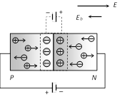
 (i) In forward biasing width of depletion layer decreases
(ii) In forward biasing resistance offered \[{{R}_{\text{Forward}}}\approx 10\Omega -25\Omega \]
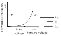
(iii) Forward bias opposes the potential barrier and for \[V>{{V}_{B}}\] a forward current is set up across the junction.
(iv) The current is given by \[i={{i}_{s}}({{e}^{eV/kT}}-1)\]; where \[{{i}_{s}}=\] Saturation current, In the exponent \[e=1.6\times {{10}^{-19}}\,C,\] \[k=\] Boltzmann's constant
(v) Cut-in (Knee) voltage : The voltage at which the current starts to increase rapidily. For Ge it is 0.3 V and for Si it is 0.7 V.
(vi) df -diffusion dr - drift
(i) In forward biasing width of depletion layer decreases
(ii) In forward biasing resistance offered \[{{R}_{\text{Forward}}}\approx 10\Omega -25\Omega \]
(iii) Forward bias opposes the potential barrier and for \[V>{{V}_{B}}\] a forward current is set up across the junction.
(iv) The current is given by \[i={{i}_{s}}({{e}^{eV/kT}}-1)\]; where \[{{i}_{s}}=\] Saturation current, In the exponent \[e=1.6\times {{10}^{-19}}\,C,\] \[k=\] Boltzmann's constant
(v) Cut-in (Knee) voltage : The voltage at which the current starts to increase rapidily. For Ge it is 0.3 V and for Si it is 0.7 V.
(vi) df -diffusion dr - drift
 (2) Reverse biasing : Positive terminal of the battery is connected to the N-crystal and negative terminal of the battery is connected to P-crystal
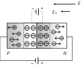 (i) In reverse biasing width of depletion layer increases
(ii) In reverse biasing resistance offered \[{{R}_{\operatorname{Re}verse}}\approx {{10}^{5}}\Omega \]
(iii) Reverse bias supports the potential barrier and no current flows across the junction due to the diffusion of the majority carriers. (A very small reverse currents may exist in the circuit due to the drifting of minority carriers across the junction)
(iv) Break down voltage : Reverse voltage at which break down of semiconductor occurs. For Ge it is 25 V and for Si it is 35 V.
(v)
(i) In reverse biasing width of depletion layer increases
(ii) In reverse biasing resistance offered \[{{R}_{\operatorname{Re}verse}}\approx {{10}^{5}}\Omega \]
(iii) Reverse bias supports the potential barrier and no current flows across the junction due to the diffusion of the majority carriers. (A very small reverse currents may exist in the circuit due to the drifting of minority carriers across the junction)
(iv) Break down voltage : Reverse voltage at which break down of semiconductor occurs. For Ge it is 25 V and for Si it is 35 V.
(v) 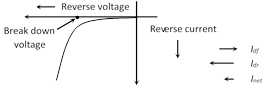
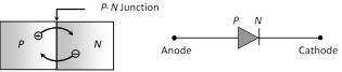 (1) Depletion region : On account of difference in concentration of charge carrier in the two sections of P-N junction, the electrons from N-region diffuse through the junction into P-region and the hole from P region diffuse into N-region.
Due to diffusion, neutrality of both N and P-type semiconductor is disturbed, a layer of negative charged ions appear near the junction in the P-crystal and a layer of positive ions appears near the junction in N-crystal. This layer is called depletion layer
(1) Depletion region : On account of difference in concentration of charge carrier in the two sections of P-N junction, the electrons from N-region diffuse through the junction into P-region and the hole from P region diffuse into N-region.
Due to diffusion, neutrality of both N and P-type semiconductor is disturbed, a layer of negative charged ions appear near the junction in the P-crystal and a layer of positive ions appears near the junction in N-crystal. This layer is called depletion layer
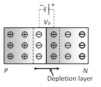 (i) The thickness of depletion layer is 1 micron \[={{10}^{-6}}\,m\].
(ii) Width of depletion layer \[\propto \frac{1}{\text{Dopping}}\]
(iii) Depletion is directly proportional to temperature.
(iv) The P-N junction diode is equivalent to capacitor in which the depletion layer acts as a dielectric.
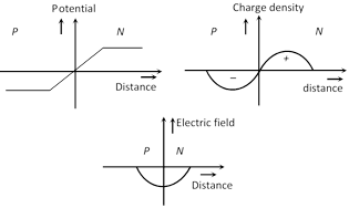
(2) Potential barrier : The potential difference created across the P-N junction due to the diffusion of electron and holes is called potential barrier. For Ge \[{{V}_{B}}=0.3V\] and for silicon \[{{V}_{B}}=0.7V\] On the average the potential barrier in P-N junction is \[\tilde{\ }0.5\,\,V\] and the width of depletion region \[\tilde{\ }{{10}^{-6}}\,m\]So the barrier electric field \[E=\frac{V}{d}=\frac{0.5}{{{10}^{-6}}}=5\times {{10}^{5}}\,V/m\]
(3) Some important graphs
(i) The thickness of depletion layer is 1 micron \[={{10}^{-6}}\,m\].
(ii) Width of depletion layer \[\propto \frac{1}{\text{Dopping}}\]
(iii) Depletion is directly proportional to temperature.
(iv) The P-N junction diode is equivalent to capacitor in which the depletion layer acts as a dielectric.
(2) Potential barrier : The potential difference created across the P-N junction due to the diffusion of electron and holes is called potential barrier. For Ge \[{{V}_{B}}=0.3V\] and for silicon \[{{V}_{B}}=0.7V\] On the average the potential barrier in P-N junction is \[\tilde{\ }0.5\,\,V\] and the width of depletion region \[\tilde{\ }{{10}^{-6}}\,m\]So the barrier electric field \[E=\frac{V}{d}=\frac{0.5}{{{10}^{-6}}}=5\times {{10}^{5}}\,V/m\]
(3) Some important graphs
 (4) Diffusion and drift current : Because of concentration difference holes/electron try to diffuse from their side to other side. Only those holes/electrons crosses the junction, which have high kinetic energy. This diffusion results in an electric current from the P-side to the N-side known as diffusion current \[({{i}_{df}})\]
As electron hole pair (because of thermal collisions) are continuously created in the depletion region. There is a regular flow of electrons towards the N-side and of holes towards the P-side. This makes a current from the N-side to the P-side. This current is called the drift current \[({{i}_{dr}})\].
(4) Diffusion and drift current : Because of concentration difference holes/electron try to diffuse from their side to other side. Only those holes/electrons crosses the junction, which have high kinetic energy. This diffusion results in an electric current from the P-side to the N-side known as diffusion current \[({{i}_{df}})\]
As electron hole pair (because of thermal collisions) are continuously created in the depletion region. There is a regular flow of electrons towards the N-side and of holes towards the P-side. This makes a current from the N-side to the P-side. This current is called the drift current \[({{i}_{dr}})\]. 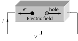 (3) As we know \[\sigma =\frac{J}{E}=\frac{i}{AE}\]. Hence conductivity of semiconductor \[\sigma =e[{{n}_{e}}{{\mu }_{e}}+{{n}_{h}}{{\mu }_{h}}]\]; where \[{{v}_{e}}=\] drift velocity of electron, \[{{v}_{h}}=\] drift velocity of holes, E = Applied electric field \[{{\mu }_{e}}=\frac{{{v}_{e}}}{E}=\] mobility of electron and \[{{\mu }_{h}}=\frac{{{v}_{h}}}{E}=\] mobility of holes
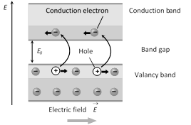
(4) Motion of electrons in the conduction band and of holes the valence band under the action of electric field is shown below
(3) As we know \[\sigma =\frac{J}{E}=\frac{i}{AE}\]. Hence conductivity of semiconductor \[\sigma =e[{{n}_{e}}{{\mu }_{e}}+{{n}_{h}}{{\mu }_{h}}]\]; where \[{{v}_{e}}=\] drift velocity of electron, \[{{v}_{h}}=\] drift velocity of holes, E = Applied electric field \[{{\mu }_{e}}=\frac{{{v}_{e}}}{E}=\] mobility of electron and \[{{\mu }_{h}}=\frac{{{v}_{h}}}{E}=\] mobility of holes
(4) Motion of electrons in the conduction band and of holes the valence band under the action of electric field is shown below
 (5) At absolute zero temperature (0 K) conduction band of semiconductor is completely empty i.e. \[\sigma =0\]. Hence the semiconductor behaves as an insulator.
 | Material | Type | Density of conduction electrons (m- 3) | Density of holes (m-3) |
| Copper | Conductor | \[9\times {{10}^{28}}\] | 0 |
| Silicon | Intrinsic semiconductor | \[7\times {{10}^{75}}\] | \[7\times {{10}^{15}}\] |
| Silicon doped with phosphorus (1 part in \[{{10}^{6}}\]) | N-type semiconductor | \[5\times {{10}^{22}}\] | \[1\times {{10}^{9}}\] |
| more...
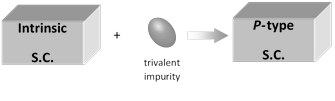
These are obtained by adding a small amount of trivalent impurity to a pure sample of semiconductor (Ge).
 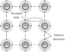 (1) Majority charge carriers - holes Minority charge carriers - electrons
(2) \[{{n}_{h}}>>{{n}_{e}};\,{{i}_{h}}>>{{i}_{e}}\]
(3) Conductivity \[\sigma ={{n}_{h}}{{\mu }_{h}}\,e\]
(4) P-type semiconductor is also electrically neutral (not positively charged)
(5) Impurity is called Acceptor impurity.
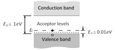
(6) Acceptor energy level lies just above the valence band.
(1) Majority charge carriers - holes Minority charge carriers - electrons
(2) \[{{n}_{h}}>>{{n}_{e}};\,{{i}_{h}}>>{{i}_{e}}\]
(3) Conductivity \[\sigma ={{n}_{h}}{{\mu }_{h}}\,e\]
(4) P-type semiconductor is also electrically neutral (not positively charged)
(5) Impurity is called Acceptor impurity.
(6) Acceptor energy level lies just above the valence band.
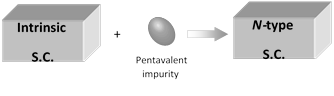
These are obtained by adding a small amount of pentavalent impurity to a pure sample of semiconductor (Ge).
 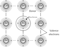 (1) Majority charge carriers - electrons Minority charge carriers - holes
(2) \[{{n}_{e}}>>{{n}_{h}};\,\,{{i}_{e}}>>{{i}_{h}}\]
(3) Conductivity \[\sigma \approx {{n}_{e}}{{\mu }_{e}}\,e\]
(4) N-type semiconductor is electrically neutral (not negatively charged)
(5) Impurity is called Donar impurity because one impurity atom generate one electron.
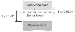
(6) Donor energy level lies just below the conduction band.
(1) Majority charge carriers - electrons Minority charge carriers - holes
(2) \[{{n}_{e}}>>{{n}_{h}};\,\,{{i}_{e}}>>{{i}_{h}}\]
(3) Conductivity \[\sigma \approx {{n}_{e}}{{\mu }_{e}}\,e\]
(4) N-type semiconductor is electrically neutral (not negatively charged)
(5) Impurity is called Donar impurity because one impurity atom generate one electron.
(6) Donor energy level lies just below the conduction band.
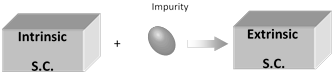
(1) An impure semiconductor is called extrinsic semiconductor
(2) When pure semiconductor material is mixed with small amounts of certain specific impurities with valency different from that of the parent material, the number of mobile electrons/holes drastically changes. The process of addition of impurity is called doping.
 (3) Pentavalent impurities : The elements whose atom has five valance electrons are called pentavalent impurities e.g. As, P, Sb etc. These impurities are also called donor impurities because they donate extra free electron.
(4) Trivalent impurities : The elements whose each atom has three valance electrons are called trivalent impurities e.g. In, Ga, Al, B, etc. These impurities are also called acceptor impurities as they accept electron.
(5) The compounds of trivalent and pentavalent elements also behaves like semiconductors e.g. GaAs, InSb, In P, GaP etc.
(6) The number of atoms of impurity element is about 1 in \[{{10}^{8}}\] atoms of the semiconductor.
(7) In extrinsic semiconductors \[{{n}_{e}}\ne {{n}_{h}}\]
(8) In extrinsic semiconductors fermi level shifts towards valence or conduction energy bands.
(9) Their conductivity is high and they are used for practical purposes.
(10) In a doped extrinsic semiconductor, the number density of \[{{e}^{-}}\]of the conduction band \[({{n}_{e}})\] and the number density of holes in the valence band \[({{n}_{h}})\] differs from that in a pure semiconductor. If \[{{n}_{i}}\] is the number density of electron in conduction band or the number density of holes in valence band in a pure semiconductor then \[{{n}_{e}}{{n}_{h}}=n_{i}^{2}\](mass action law)
(11) Extrinsic semiconductors are of two types
(i) N-type semiconductor
(ii) P-type semiconductor
(3) Pentavalent impurities : The elements whose atom has five valance electrons are called pentavalent impurities e.g. As, P, Sb etc. These impurities are also called donor impurities because they donate extra free electron.
(4) Trivalent impurities : The elements whose each atom has three valance electrons are called trivalent impurities e.g. In, Ga, Al, B, etc. These impurities are also called acceptor impurities as they accept electron.
(5) The compounds of trivalent and pentavalent elements also behaves like semiconductors e.g. GaAs, InSb, In P, GaP etc.
(6) The number of atoms of impurity element is about 1 in \[{{10}^{8}}\] atoms of the semiconductor.
(7) In extrinsic semiconductors \[{{n}_{e}}\ne {{n}_{h}}\]
(8) In extrinsic semiconductors fermi level shifts towards valence or conduction energy bands.
(9) Their conductivity is high and they are used for practical purposes.
(10) In a doped extrinsic semiconductor, the number density of \[{{e}^{-}}\]of the conduction band \[({{n}_{e}})\] and the number density of holes in the valence band \[({{n}_{h}})\] differs from that in a pure semiconductor. If \[{{n}_{i}}\] is the number density of electron in conduction band or the number density of holes in valence band in a pure semiconductor then \[{{n}_{e}}{{n}_{h}}=n_{i}^{2}\](mass action law)
(11) Extrinsic semiconductors are of two types
(i) N-type semiconductor
(ii) P-type semiconductor
(1) A pure semiconductor is called intrinsic semiconductor. It has thermally generated current carriers
(2) They have four electrons in the outermost orbit of atom and atoms are held together by covalent bond
(3) Free electrons and holes both are charge carriers and \[{{n}_{e}}\](in C.B.) \[={{n}_{h}}\](in V.B.)
(4) The drift velocity of electrons \[({{v}_{e}})\]is greater than that of holes\[({{v}_{h}})\]
(5) For them fermi energy level lies at the centre of the C.B. and V.B.
(6) In pure semiconductor, impurity must be less than 1 in \[{{10}^{8}}\] parts of semiconductor.
(7) In intrinsic semiconductor \[n_{e}^{(o)}=n_{h}^{(o)}={{n}_{i}}\]; where \[n_{e}^{(o)}=\] Electron density in conduction band, \[n_{h}^{(o)}=\] Hole density in V.B., \[{{n}_{i}}=\] Density of intrinsic carriers.
(8) The fraction of electrons of valance band present in conduction band is given by \[f\propto {{e}^{-{{E}_{g}}/kT}}\]; where \[{{E}_{g}}=\] Fermi energy or k = Boltzmann's constant and T = Absolute temperature
(9) Because of less number of charge carriers at room temperature, intrinsic semiconductors have low conductivity so they have no practical use.
(10) Number of electrons reaching from valence band to conduction band \[n=A{{T}^{3/2}}{{e}^{-{{E}_{g}}/2kT}}\]
(1) When an electron is removed from a covalent bond, it leaves a vacancy behind. An electron from a neighbouring atom can move into this vacancy, leaving the neighbour with a vacancy. In this way the vacancy formed is called hole (or cotter), and can travel through the material and serve as an additional current carriers.
(2) A hole is considered as a seat of positive charge, having magnitude of charge equal to that of an electron.
(3) Holes acts as virtual charge, although there is no physical charge on it.
(4) Effective mass of hole is more than electron.
(5) Mobility of hole is less than electron.
Current Affairs CategoriesArchive
Trending Current Affairs


You need to login to perform this action. |