 where \[v=\] frequency (revolution per sec) and T = Time period.
(2) Cycle wheel : A conducting wheel each spoke of length \[l\] is rotating with angular velocity \[\omega \] in a given magnetic field as shown below in fig.
Due to flux cutting each metal spoke becomes identical cell of emf e (say), all such identical cells connected in parallel fashion \[{{e}_{net}}=e\] (emf of single cell). Let N be the number of spokes hence \[{{e}_{net}}=\frac{1}{2}Bw{{l}^{2}};\,\omega =2\pi \nu \]
where \[v=\] frequency (revolution per sec) and T = Time period.
(2) Cycle wheel : A conducting wheel each spoke of length \[l\] is rotating with angular velocity \[\omega \] in a given magnetic field as shown below in fig.
Due to flux cutting each metal spoke becomes identical cell of emf e (say), all such identical cells connected in parallel fashion \[{{e}_{net}}=e\] (emf of single cell). Let N be the number of spokes hence \[{{e}_{net}}=\frac{1}{2}Bw{{l}^{2}};\,\omega =2\pi \nu \]
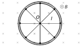 Here \[{{e}_{net}}\propto {{N}^{o}}\] i.e. total emf does not depends on number of spokes 'N'.
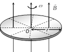
(3) Faraday copper disc generator : A metal disc can be assumed to made of uncountable radial conductors when metal disc rotates in transverse magnetic field these radial conductors cuts away magnetic field lines and because of this flux cutting all becomes identical cells each of emf 'e' where \[e=\frac{1}{2}B\omega {{r}^{2}},\]
Here \[{{e}_{net}}\propto {{N}^{o}}\] i.e. total emf does not depends on number of spokes 'N'.
(3) Faraday copper disc generator : A metal disc can be assumed to made of uncountable radial conductors when metal disc rotates in transverse magnetic field these radial conductors cuts away magnetic field lines and because of this flux cutting all becomes identical cells each of emf 'e' where \[e=\frac{1}{2}B\omega {{r}^{2}},\]
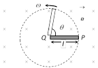
 (4) Semicircular conducting loop : If a semi-circular conducting loop (ACD) of radius 'r' with centre at O, the plane of loop being in the plane of paper. The loop is now made to rotate with a constant angular velocity \[\omega \], about an axis passing through O and perpendicular to the plane of paper. The effective resistance of the loop is R.
 In time t the area swept by the loop in the field i.e. region II \[A=\frac{1}{2}r(r\theta )=\frac{1}{2}{{r}^{2}}\omega \,t\]; \[\frac{dA}{dt}=\frac{{{r}^{2}}\omega }{2}\]
Flux link with the rotating loop at time t \[\varphi =BA\]
Hence induced emf in the loop in magnitude \[|e|=\frac{d\varphi }{dt}=B\frac{dA}{dt}=\frac{B\omega {{r}^{2}}}{2}\] and induced current \[i=\frac{|e|}{R}=\frac{B\omega {{r}^{2}}}{2R}\]
In time t the area swept by the loop in the field i.e. region II \[A=\frac{1}{2}r(r\theta )=\frac{1}{2}{{r}^{2}}\omega \,t\]; \[\frac{dA}{dt}=\frac{{{r}^{2}}\omega }{2}\]
Flux link with the rotating loop at time t \[\varphi =BA\]
Hence induced emf in the loop in magnitude \[|e|=\frac{d\varphi }{dt}=B\frac{dA}{dt}=\frac{B\omega {{r}^{2}}}{2}\] and induced current \[i=\frac{|e|}{R}=\frac{B\omega {{r}^{2}}}{2R}\] 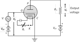 (2) The voltage at grid is the sum of signal \[{{V}_{i}}\] and grid bias \[{{V}_{gg}}\]. \[{{V}_{g}}={{V}_{gg}}+{{V}_{i}}\]
(3) Small change in grid voltage results in a large change in plate current so results in a large change in voltage across \[{{R}_{L}}\,({{V}_{0}}={{i}_{p}}{{R}_{L}}\,\Rightarrow \,\Delta {{V}_{0}}=\Delta {{i}_{p}}{{R}_{L}})\]
(4) The linear portion of the mutual characteristic with maximum slope is chosen for amplification without distortion.
(2) The voltage at grid is the sum of signal \[{{V}_{i}}\] and grid bias \[{{V}_{gg}}\]. \[{{V}_{g}}={{V}_{gg}}+{{V}_{i}}\]
(3) Small change in grid voltage results in a large change in plate current so results in a large change in voltage across \[{{R}_{L}}\,({{V}_{0}}={{i}_{p}}{{R}_{L}}\,\Rightarrow \,\Delta {{V}_{0}}=\Delta {{i}_{p}}{{R}_{L}})\]
(4) The linear portion of the mutual characteristic with maximum slope is chosen for amplification without distortion.
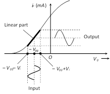 (i) For the positive half cycle of input voltage \[({{V}_{i}})\] : \[{{V}_{g}}\] becomes less negative, so \[{{i}_{p}}\] increases
(ii) For the negative half cycle of input voltage \[({{V}_{i}})\] : \[{{V}_{g}}\] becomes more negative, so \[{{i}_{p}}\] decreases
(iii) The phase difference between the output signal and input signal is \[{{180}^{o}}\] (or \[\pi \])
(5) Voltage amplification
(i) For the positive half cycle of input voltage \[({{V}_{i}})\] : \[{{V}_{g}}\] becomes less negative, so \[{{i}_{p}}\] increases
(ii) For the negative half cycle of input voltage \[({{V}_{i}})\] : \[{{V}_{g}}\] becomes more negative, so \[{{i}_{p}}\] decreases
(iii) The phase difference between the output signal and input signal is \[{{180}^{o}}\] (or \[\pi \])
(5) Voltage amplification
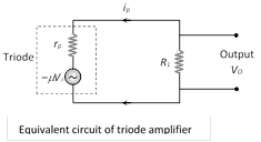 Current through the load resistance is given by \[{{i}_{p}}=-\frac{\mu {{V}_{i}}}{{{r}_{p}}+{{R}_{L}}}\,\] \[\Rightarrow \,{{V}_{0}}={{i}_{p}}{{R}_{L}}=\frac{-\,\mu {{V}_{i}}{{R}_{L}}}{{{r}_{p}}+{{R}_{L}}}\] \[\Rightarrow \] Voltage gain \[=\frac{{{V}_{0}}}{{{V}_{i}}}=-\frac{\mu {{R}_{L}}}{{{r}_{p}}+{{R}_{L}}}\] Numerically \[A=\frac{\mu {{R}_{L}}}{{{r}_{p}}+{{R}_{L}}}=\frac{\mu }{1+\frac{{{r}_{p}}}{{{R}_{L}}}}\]
(i) If \[{{R}_{L}}=\,\,\infty \,\,\Rightarrow A\] will be maximum and \[{{A}_{\max }}=\mu \] (Practically \[A<\mu \])
(ii) If \[{{r}_{p}}={{R}_{L}}\Rightarrow A=\frac{\mu }{2}\]
(iii) Power at load resistance \[P={{i}_{p}}{{V}_{0}}=i_{p}^{2}{{R}_{L}}\]
Condition for maximum power \[{{R}_{L}}={{r}_{p}}\] \[\therefore \] \[{{P}_{\max }}={{\left( \frac{\mu {{V}_{i}}}{{{R}_{L}}+{{R}_{L}}} \right)}^{2}}\times {{R}_{L}}=\frac{{{\mu }^{2}}V_{i}^{2}}{4{{R}_{L}}}\]
Current through the load resistance is given by \[{{i}_{p}}=-\frac{\mu {{V}_{i}}}{{{r}_{p}}+{{R}_{L}}}\,\] \[\Rightarrow \,{{V}_{0}}={{i}_{p}}{{R}_{L}}=\frac{-\,\mu {{V}_{i}}{{R}_{L}}}{{{r}_{p}}+{{R}_{L}}}\] \[\Rightarrow \] Voltage gain \[=\frac{{{V}_{0}}}{{{V}_{i}}}=-\frac{\mu {{R}_{L}}}{{{r}_{p}}+{{R}_{L}}}\] Numerically \[A=\frac{\mu {{R}_{L}}}{{{r}_{p}}+{{R}_{L}}}=\frac{\mu }{1+\frac{{{r}_{p}}}{{{R}_{L}}}}\]
(i) If \[{{R}_{L}}=\,\,\infty \,\,\Rightarrow A\] will be maximum and \[{{A}_{\max }}=\mu \] (Practically \[A<\mu \])
(ii) If \[{{r}_{p}}={{R}_{L}}\Rightarrow A=\frac{\mu }{2}\]
(iii) Power at load resistance \[P={{i}_{p}}{{V}_{0}}=i_{p}^{2}{{R}_{L}}\]
Condition for maximum power \[{{R}_{L}}={{r}_{p}}\] \[\therefore \] \[{{P}_{\max }}={{\left( \frac{\mu {{V}_{i}}}{{{R}_{L}}+{{R}_{L}}} \right)}^{2}}\times {{R}_{L}}=\frac{{{\mu }^{2}}V_{i}^{2}}{4{{R}_{L}}}\] 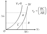 (ii) It is expressed in kilo ohms \[(K\Omega )\]. Typically, it ranges from \[8K\Omega \] to\[40K\Omega \]. The \[{{r}_{P}}\] can be determined from plate characteristics. It represents the reciprocal of the slope of the plate characteristic curve. (iii) If the distance between plate and cathode is increased the \[{{r}_{P}}\] increases. The value of \[{{r}_{P}}\] is infinity in the state of cut off bias or saturation state.
(2) Mutual conductance (or trans conductance) \[({{g}_{m}})\]
(i) It is defined as the ratio of small change in plate current \[(\Delta {{i}_{p}})\] to the corresponding small change in grid potential \[(\Delta {{V}_{g}})\] when plate potential \[{{V}_{p}}\] is kept constant i.e. \[{{g}_{m}}={{\left( \frac{\Delta {{i}_{p}}}{\Delta {{V}_{g}}} \right)}_{{{V}_{p\,}}\text{is}\,\text{constant}}}\]
(ii) It is expressed in kilo ohms \[(K\Omega )\]. Typically, it ranges from \[8K\Omega \] to\[40K\Omega \]. The \[{{r}_{P}}\] can be determined from plate characteristics. It represents the reciprocal of the slope of the plate characteristic curve. (iii) If the distance between plate and cathode is increased the \[{{r}_{P}}\] increases. The value of \[{{r}_{P}}\] is infinity in the state of cut off bias or saturation state.
(2) Mutual conductance (or trans conductance) \[({{g}_{m}})\]
(i) It is defined as the ratio of small change in plate current \[(\Delta {{i}_{p}})\] to the corresponding small change in grid potential \[(\Delta {{V}_{g}})\] when plate potential \[{{V}_{p}}\] is kept constant i.e. \[{{g}_{m}}={{\left( \frac{\Delta {{i}_{p}}}{\Delta {{V}_{g}}} \right)}_{{{V}_{p\,}}\text{is}\,\text{constant}}}\]
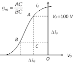 (ii) The value of \[{{g}_{m}}\] is equal to the slope of mutual characteristics of triode.
(iii) The value of \[{{g}_{m}}\] depends upon the separation between grid and cathode. The smaller is this separation, the larger is the value of \[{{g}_{m}}\] and vice versa. (iv) In the saturation state, the value of \[\Delta {{i}_{p}}=0\], \[{{g}_{m}}=0\]
(3) Amplification factor \[(\mu )\] : It is defined as the ratio of change in plate potential \[(\Delta {{V}_{p}})\] to produce certain change in plate current \[(\Delta {{i}_{p}})\] to the change in grid potential \[(\Delta {{V}_{g}})\] for the same change in plate current \[(\Delta {{i}_{p}})\]i.e. \[\mu =-\,{{\left( \frac{\Delta {{V}_{p}}}{\Delta {{V}_{g}}} \right)}_{\Delta {{I}_{p}}=\,\text{a constant }}}\]; negative sign indicates that \[{{V}_{p}}\] and \[{{V}_{g}}\] are in opposite phase. (i) Amplification factor depends upon the distance between plate and cathode \[({{d}_{pk}}),\] plate and grid \[{{d}_{pg}}\] and grid and cathode \[({{d}_{gk}})\]. i.e. \[\mu \,\propto \,{{d}_{pg}}\propto \,{{d}_{pk}}\propto \frac{1}{{{d}_{gk}}}\] (ii) The value of \[\mu \] is greater than one. (iii) Amplification factor is unitless and dimensionless.
(4) Relation between triode constants : The triode constants are not independent of each other. They are related by the relation \[\mu ={{r}_{p}}\times {{g}_{m}}\] The \[{{r}_{p}}\] and \[{{g}_{m}}\] depends on \[{{i}_{p}}\] in the following manner \[{{r}_{p}}\propto {{i}_{p}}^{-1/3}\], \[{{g}_{m}}\propto {{i}_{p}}^{1/3}\], \[\mu \] does not depend on \[{{i}_{p}}\].
Above three constants may be determined from any one set of characteristic curves.
(ii) The value of \[{{g}_{m}}\] is equal to the slope of mutual characteristics of triode.
(iii) The value of \[{{g}_{m}}\] depends upon the separation between grid and cathode. The smaller is this separation, the larger is the value of \[{{g}_{m}}\] and vice versa. (iv) In the saturation state, the value of \[\Delta {{i}_{p}}=0\], \[{{g}_{m}}=0\]
(3) Amplification factor \[(\mu )\] : It is defined as the ratio of change in plate potential \[(\Delta {{V}_{p}})\] to produce certain change in plate current \[(\Delta {{i}_{p}})\] to the change in grid potential \[(\Delta {{V}_{g}})\] for the same change in plate current \[(\Delta {{i}_{p}})\]i.e. \[\mu =-\,{{\left( \frac{\Delta {{V}_{p}}}{\Delta {{V}_{g}}} \right)}_{\Delta {{I}_{p}}=\,\text{a constant }}}\]; negative sign indicates that \[{{V}_{p}}\] and \[{{V}_{g}}\] are in opposite phase. (i) Amplification factor depends upon the distance between plate and cathode \[({{d}_{pk}}),\] plate and grid \[{{d}_{pg}}\] and grid and cathode \[({{d}_{gk}})\]. i.e. \[\mu \,\propto \,{{d}_{pg}}\propto \,{{d}_{pk}}\propto \frac{1}{{{d}_{gk}}}\] (ii) The value of \[\mu \] is greater than one. (iii) Amplification factor is unitless and dimensionless.
(4) Relation between triode constants : The triode constants are not independent of each other. They are related by the relation \[\mu ={{r}_{p}}\times {{g}_{m}}\] The \[{{r}_{p}}\] and \[{{g}_{m}}\] depends on \[{{i}_{p}}\] in the following manner \[{{r}_{p}}\propto {{i}_{p}}^{-1/3}\], \[{{g}_{m}}\propto {{i}_{p}}^{1/3}\], \[\mu \] does not depend on \[{{i}_{p}}\].
Above three constants may be determined from any one set of characteristic curves.
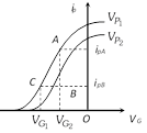 \[{{r}_{p}}=\frac{{{V}_{P1}}-{{V}_{P2}}}{{{I}_{PA}}-{{I}_{PB}}}\], \[{{g}_{m}}=\frac{{{I}_{PA}}-{{I}_{PB}}}{{{V}_{G1}}-{{V}_{G2}}}\], \[\mu =-\frac{{{V}_{P1}}-{{V}_{P2}}}{{{V}_{G2}}-{{V}_{G1}}}\]
 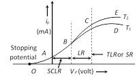 The curve is not linear hence diode valve is a non-ohmic device.
(1) Space charge limited region (SCLR) : In this region current is space charge limited current.
Also \[{{i}_{p}}\,\propto \,V_{p}^{3/2}\]\[\Rightarrow \]\[{{i}_{p}}=kV_{p}^{3/2}\]; where k is a constant depending on metal as well as on the shape and area of the cathode. This is called child?s law.
(2) Linear region (LR) : In this region \[{{i}_{p}}\,\propto \,{{V}_{p}}\]
(3) Saturated region (SR) or temperature limited region (TLR) : In this part, the current is independent of potential difference applied between the cathode and anode. \[{{i}_{p}}\ne f({{V}_{p}})\], \[{{i}_{p}}=f\] (Temperature) The saturation current follows Richardson Dushman equation i.e. \[i=AS{{T}^{2}}{{e}^{-{{\varphi }_{0}}/kT}}\]; Here A = Emission constant =\[\frac{4\pi \ me{{k}^{2}}}{{{h}^{3}}}amp/{{m}^{2}}-{{k}^{2}}\] S = Area of emitter in \[{{m}^{2}}\]; T = Absolute temperature in K \[{{\varphi }_{0}}\]= Work function of metal in Joule; k =Boltzmann constant The small increase in \[{{i}_{p}}\] after saturation stage due to field emission is known as Shottkey effect.
(4) Diode resistance
(i) Static plate resistance or dc plate resistance : \[{{R}_{p}}=\frac{{{V}_{p}}}{{{i}_{p}}}\].
(ii) Dynamic or ac plate resistance : If at constant filament current, a small change \[\Delta {{V}_{P}}\] in the plate potential produces a small change \[\Delta {{i}_{p}}\] in the plate current, then the ratio \[\Delta {{V}_{p}}/\Delta {{i}_{p}}\] is called the dynamic resistance, or the 'plate resistance' of the diode \[{{r}_{p}}=\frac{\Delta {{V}_{p}}}{\Delta {{i}_{p}}}\].
(iii) In SCLR : \[{{r}_{p}}<{{R}_{p}}\],
(iv) In TLR :\[{{R}_{p}}<{{r}_{p}}\] and \[{{r}_{p}}=\infty \].
(5) Uses of diode valve
(i) As a rectifier
(ii) As a detector
(iii) As a transmitter
(iv) As a modulator
The curve is not linear hence diode valve is a non-ohmic device.
(1) Space charge limited region (SCLR) : In this region current is space charge limited current.
Also \[{{i}_{p}}\,\propto \,V_{p}^{3/2}\]\[\Rightarrow \]\[{{i}_{p}}=kV_{p}^{3/2}\]; where k is a constant depending on metal as well as on the shape and area of the cathode. This is called child?s law.
(2) Linear region (LR) : In this region \[{{i}_{p}}\,\propto \,{{V}_{p}}\]
(3) Saturated region (SR) or temperature limited region (TLR) : In this part, the current is independent of potential difference applied between the cathode and anode. \[{{i}_{p}}\ne f({{V}_{p}})\], \[{{i}_{p}}=f\] (Temperature) The saturation current follows Richardson Dushman equation i.e. \[i=AS{{T}^{2}}{{e}^{-{{\varphi }_{0}}/kT}}\]; Here A = Emission constant =\[\frac{4\pi \ me{{k}^{2}}}{{{h}^{3}}}amp/{{m}^{2}}-{{k}^{2}}\] S = Area of emitter in \[{{m}^{2}}\]; T = Absolute temperature in K \[{{\varphi }_{0}}\]= Work function of metal in Joule; k =Boltzmann constant The small increase in \[{{i}_{p}}\] after saturation stage due to field emission is known as Shottkey effect.
(4) Diode resistance
(i) Static plate resistance or dc plate resistance : \[{{R}_{p}}=\frac{{{V}_{p}}}{{{i}_{p}}}\].
(ii) Dynamic or ac plate resistance : If at constant filament current, a small change \[\Delta {{V}_{P}}\] in the plate potential produces a small change \[\Delta {{i}_{p}}\] in the plate current, then the ratio \[\Delta {{V}_{p}}/\Delta {{i}_{p}}\] is called the dynamic resistance, or the 'plate resistance' of the diode \[{{r}_{p}}=\frac{\Delta {{V}_{p}}}{\Delta {{i}_{p}}}\].
(iii) In SCLR : \[{{r}_{p}}<{{R}_{p}}\],
(iv) In TLR :\[{{R}_{p}}<{{r}_{p}}\] and \[{{r}_{p}}=\infty \].
(5) Uses of diode valve
(i) As a rectifier
(ii) As a detector
(iii) As a transmitter
(iv) As a modulator 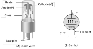 (1) Inventor : Fleming
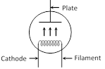
(2) Principle : Thermionic emission
(3) Number of electrodes : Two
(4) Working : When plate potential \[({{V}_{p}})\] is positive, plate current\[({{i}_{p}})\] flows in the circuit (because some emitted electrons reaches to plate). If \[+{{V}_{p}}\] increases \[{{i}_{p}}\] also increases and finally becomes maximum (saturation).
(1) Inventor : Fleming
(2) Principle : Thermionic emission
(3) Number of electrodes : Two
(4) Working : When plate potential \[({{V}_{p}})\] is positive, plate current\[({{i}_{p}})\] flows in the circuit (because some emitted electrons reaches to plate). If \[+{{V}_{p}}\] increases \[{{i}_{p}}\] also increases and finally becomes maximum (saturation).
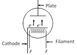
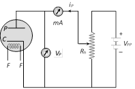 (5) Space charge : If \[{{V}_{p}}\]is zero or negative, then electrons collect around the plate as a cloud which is called space charge. space charge decreases the emission of electrons from the cathode.
 | Directly heated emitter | Indirectly heated emitter |
 |
 |
| Cathode is directly heated by passing current. | Cathode is indirectly heated. |
| Thermionic current is less. | Thermionic current is more. |
| Energy consumption and life is small. | Energy consumption and life is more. |
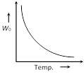
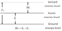 Work function for different materials \[{{({{W}_{0}})}_{\text{Pure tungsten}}}\text{ }\!\!~\!\!\text{ }~=\text{ }4.5eV\]
\[{{({{W}_{0}})}_{\text{Throated tungsten}}}~=\text{ }2.6eV\] \[{{({{W}_{0}})}_{\text{Oxide coated tungsten}}}=\text{ }1eV\]
Work function for different materials \[{{({{W}_{0}})}_{\text{Pure tungsten}}}\text{ }\!\!~\!\!\text{ }~=\text{ }4.5eV\]
\[{{({{W}_{0}})}_{\text{Throated tungsten}}}~=\text{ }2.6eV\] \[{{({{W}_{0}})}_{\text{Oxide coated tungsten}}}=\text{ }1eV\]
 (5) Four processes of electron emission from a metal are
(i) Thermionic emission
(ii) Photoelectric emission
(iii) Field emission
(iv) Secondary emission
(5) Four processes of electron emission from a metal are
(i) Thermionic emission
(ii) Photoelectric emission
(iii) Field emission
(iv) Secondary emission 


You need to login to perform this action.
You will be redirected in
3 sec

