A) AND gate
B) NAND gate
C) NOR gate
D) OR gate
Correct Answer: C
Solution :
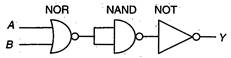
The gate circuit can be shown by giving two inputs A and B.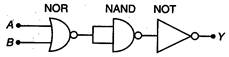 Output of NOR gate, \[{{Y}_{1}}=\overline{A+B}\] Output of NAND gate, \[{{Y}_{2}}=\overline{{{Y}_{1}}.{{Y}_{1}}}\] \[=\overline{\overline{A+B}.\overline{A+B}}\] \[=\overline{\overline{A+B}}+\overline{\overline{A+B}}\] \[=(A+B)+(A+B)\] \[=A+B\] Output of NOT gate, \[=Y=\overline{{{Y}_{2}}}\] \[=\overline{A+B}\] which is the output of NOR gate. Alternative:
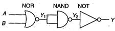
| NOR | NAND | NOT | ||||
| A | B | \[{{Y}_{1}}\] | \[{{Y}_{1}}\] | \[{{Y}_{1}}\] | \[{{Y}_{2}}\] | Y |
| 0 | 0 | 1 | 1 | 1 | 0 | 1 |
| 0 | 1 | 0 | 0 | 0 | 1 | 0 |
| 1 | 0 | 0 | 0 | 0 | 1 | 0 |
| 1 | 1 | 0 | 0 | 0 | 1 | 0 |


You need to login to perform this action.
You will be redirected in
3 sec

