Basic Electronics
Category : Railways
Basic Electronics
Electronics is considered to be a branch of Physics and Electrical engineering, Electronics is the science of controlling electrical energy electrically, in which the electrons have a fundamental role. Electronics deals with electrical circuits that involve active
Electrical components such as vacuum tubes, transistors, diodes, migrated circuits, associated passive electrical components, and interconnection technologies. Commonly, electronic devices contain circuitry consisting primarily or exclusively of active semiconductors supplemented with passive elements; such a circuit is described as an electronic circuit.
Industrial Electronics
Insustrial electronics is a branch of electronics that deals with power electronic devices such as thyristors, SCRs, AC/DC drives, meters, sensors, analyzers, load cells automatic test equipment, multi-meters, data recorders, relays, resistors, semiconductors, transistors, waveguides, scopes, amplifiers, radio frequency (RF) circuit boards, timers, counters, etc. It covers all of the methods
And facets of: control systems, instrumentation, mechanism and diagnosis, signal processing and automation of various industrial applications. The core research areas of industrial electronics include electrical power machine designs, power conditioning and power semiconductor devices, A lot of consideration is given to power economy and energy management in consumer electronic products.
The scope of industrial electronics ranges from the design and maintenance of simple electrical fuses to complicated programmable logic controllers (PLCs), solid-state devices and drives. Industrial electronics can handle the automation of all types of modem day electrical and mechanical industrial processes, Some of the specialty equipment used in industrial electronics includes: variable frequency converter and inverter drives, human machine interfaces, hydraulic, positioners and computer or microprocessor controlled robotics.
Electronic Components and Their Functions
Electronic tube or Vacuum tube
Vacuum tube is a device that controls electric current between electrodes in an evacuated container. The concept of thermionic valve or vacuum tubes used the idea that a heated element in a vacuum emitted electrons that would normally remain in the vicinity of this heated element because of the charge attraction.
If a second electrode was placed into the vacuum and a high positive potential placed on it, then the electrons would be attracted away from the heated element towards this element with a high potential. As a result a current would flow in this direction.
As electrons were unable to travel in the reverse direction, this simple valve or vacuum tube acts as a diode.
It is also possible to place a third element known as a grid into the structure between the structure between the other two electrodes. This electrode is normally formed of a gauze to allow electrons to pass through. By varying the potential on this electrode, the flow of electrons can be controlled. There are a number of electrodes in a valve or vacuum tube:
SEMICONDUCTORS
The matrials that are neither conductor nor insulator with energy gap of about 1 eV (electron volt) are called semiconductors.
Most common type of materials that are commercially used as semiconductors are germanium (Ge) and silicon (Si) because of their property to with stand high temperature.
That means there will be no significant change in energy gap with changing temperature.
Germanium and silicon are used most frequently in electronics and transistor manufacturing. Both the elements have same crystal structure and similar characteristics.
Intrinsic Semiconductors
Semiconductor is an intrinsic semiconductor when its in pure form is called as intrinsic semiconductor.
In pure semiconductor number of electrons (n) is equal to number of holes (p) and thus conductivity is very low as valence electrons are covalent bonded.
In this case we write n=p=ni, where ni is called the intrinsic concentration.
It can be shown that ni can be written
\[{{n}_{i}}={{n}_{0}}T\,\,\frac{2}{3}\,\,e\,\,\frac{{{V}_{G}}}{2{{V}_{T}}}\]
Where,\[{{n}_{0}}\]is a constant.
T is the absolute temperature.
\[{{V}_{G}}\]is the semiconductor band gap voltage.
\[{{V}_{T}}\]is the thermal voltage.
The thermal voltage is related to the temperature by
\[{{V}_{TQ}}=kT/q\]
Where, k is the Boltzmann constant \[(k=1.381\times {{10}^{-23}}J/K)\]
Extrinsic Semiconductors
Semiconductor is an extrinsic semiconductor when it's in impure form is called extrinsic semiconductors.
Extrinsic semiconductor is one that has been doped, that is, into which a doping agent has been introduced, giving it different electrical properties than the intrinsic (pure) semiconductor.
This doping involves adding dopant atoms to an intrinsic semiconductor, which changes the electron and hole carrier concentrations of the semiconductor at thermal equilibrium, the temperature at which two adjacent substances exchange no heat energy
Extrinsic semiconductor is formed by adding a small amount of impurity.
Depending on the type of impurity added we have two types of semiconductors: N - type and P-type semiconductors.
In 100 million parts of semiconductor one part of impurity is added.
N type Semiconductor
In N type semiconductor, majority carriers are electrons and minority carriers are holes.
N – type semiconductor is formed by adding penta-valent (five valence electrons) impurity in pure semiconductor crystal, e.g. As, Sb
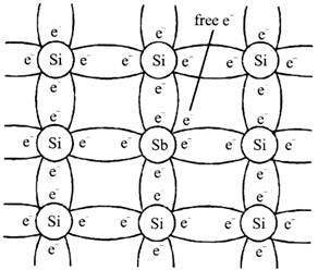
Four of the five valence electron of penta-valent impurity forms covalent bond with Si atom and the remaining electron is free to move anywhere within the crystal.
Penta-valent impurity donates electron to Si that's why N-type impurity atoms are known as donor atoms.
This enhances the conductivity of pure Si.
Majority carriers are electrons therefore conductivity is due to these electrons only and is given by, \[\sigma =ne{{\mu }_{e}}\]
P – type Semiconductors
In P-type of semiconductor, majority carriers are holes an minority carriers are electrons.
P- Type semiconductor is formed by adding trivalent (three valence electrons) impurity in pure semiconductor crystal, e.g. B, Al.
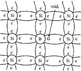
Three of the four valence electron of tetravalent impurity forms covalent bond with Si atom.
This leaves an empty space which is referred to as hole. When temperature is raised electron from another covalent bond jump to fill this empty space. This leaves a hole behind. In this way conduction takes place.
P – Type impurity accepts electron and is called acceptor atom. Majority carriers are holes and therefore conductivity is due to these holes only and is given by, \[\sigma =ne{{\mu }_{h}}\]
TRANSISTOR
A transistor is .a semiconductor device used to amplify the electronic signals and switching circuits. It is composed of semiconductor material usually with at least three terminals connection to an external circuit such as emitter (E), Base (B) and Collector (C) for connections with other components in the circuit Some transistors contains fourth terminal also i.e. substrate (S) Transistor is one of the active components. From the time of fir transistor invention to present days, either holes or electrons are responsible for the conduction of transistors.
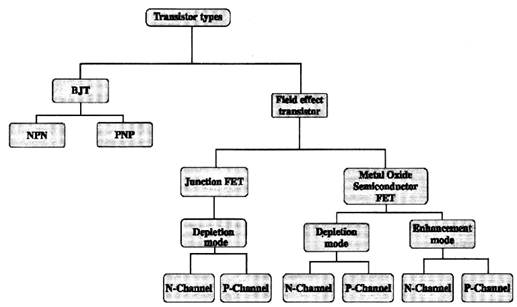
The transistors are classified into different types depending either construction or operation, they are explained using tree diagram as below.
The transistors classification can be understood by observing the bellow tree diagram. Transistors are basically classified in two types;
They are Bipolar Junction Transistors (BJT) and Field Effect Transistors (FET) or uni-polar. The BJTs are again classified into NPN and PNP transistors. The FET transistors are classified into JFET and MOSFET.
BJT
Bipolar Junction Transistor (BJT) is a Semiconductor device constructed with three doped Semiconductor Regions (Base, Collector and Emitter) separated by two p-n Junctions, Figure 1.
The p-n Junction between the Base and the Emitter has a Barrier Voltage \[({{V}_{0}})\] of about 0.6 V, which is an important parameter of a BJT, Unlike the Field Effect Transistor (FET), in which Current is produced only by one type of Charge Carrier (Electrons or Holes), in BJT, Current is produced by both types of Charge Carriers (Electrons and Holes), hence the name Bipolar.
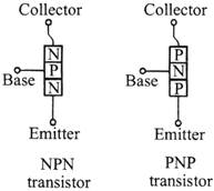
There are two Types of BJT: npn and pnp. The npn Type consists of two n-Regions separated by a p-Region. The pnp Type consists of two p-Regions separated by an n-Region.
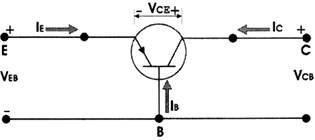
N-P- Bipolar junction transistor
In the operation of n-p-n bipolar transistor one p – type semiconductor resides between two n-type semiconductors the diagram below a n-p-n transistor is shown.
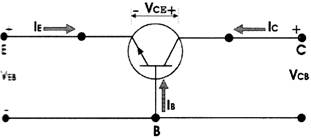
As electrons are the majority carriers in n region, these electrons on being forward bias by the voltage \[{{V}_{EB}}\] crosses the junction and appears in the base region.
A few electrons combine with the holes in p-region and are lost as charge carries. This produces the base region.
Now, the electrons in the n-region are readily swept up by the positive collector voltage\[{{V}_{CB}}\]
In this way, the collectors current build up in the direction opposite to that of flow of electrons.
Now see \[{{I}_{C}}{{I}_{E}}\]are the collect current and emitter current respectively and \[{{V}_{EB}}\] and \[{{V}_{CB}}\] are emitter base voltage and collector base voltage respectively. According to convention if for the emitter, base and collector current ie, ib and Ic current goes into the transistor the sign of the current is taken as positive and if current goes out from the transistor then the sign is taken as negative.
From KCL, it is clear that the emitter current is equal to the base and collector currents.
i.e, \[{{I}_{E}}={{I}_{B}}+{{I}_{C}}\]
Where \[{{I}_{E}}=Emitter\,\,current\]
ib = base current. \[{{I}_{B}}=base\,\,current\]
\[{{I}_{C}}\]= collector currents.
P – N – P Bipolar Junction Transistor
Similarly for \[pnp\]bipolar junction transistor one n-type semiconductors are sandwiched between two p-type semiconductors. The diagram of a \[pnp\]transistor is shown below
the emitter terminal. Like any bipolar junction transistor, the emitter-base junction is forward biased and the collector-base junction is reverse biased.
From KCL, it is clear that the collector current is equal to the difference between emitter current and base current.
i.e., \[{{I}_{C}}={{I}_{E}}-{{I}_{B}}\]
\[{{I}_{E}}={{I}_{B}}+{{I}_{C}}\]
Where \[{{I}_{E}}\]=emitter current
\[{{I}_{B}}\] =base current
\[{{I}_{C}}\]=collector currents
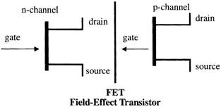
FIELD EFFECT TRANSISTORS
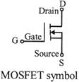
The Field–Effect–Transistor(FET)is another transistors type Basically the FET transistors have three terminals they are gate (G), Drain (D) and Source (S). FET transistors are classified into Junction Field Effect transistors (JFET) and Insulated Gate FET\[(IG-FET)\] or MOSFET transistors.
For the connections in the circuit we also consider fourth terminal called base or substrate.
The FET transistors have control on the size and shape of a channel between source and drain which is created by applied voltage.
The FET transistors are uni-polar transistors because they perform single channel operation where as BJT transistors are bipolar junction transistors.
The FET transistors have high current gain than BJT transistors. Field Effect transistors have very high input impedance, from several mega ohms \[(M\Omega )\]of resistance to much, much larger values. This high input impedance causes them to have very little current run through them. According to ohm's law, current is inversely affected by the value of the impedance of the circuit.
If the impedance is high, the current is very low.
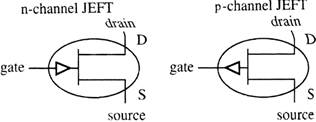
JUNCTION FIELD EFFECT TRANSISTORS
JFET:- The Junction field effect transistors like BJTs are three lead semiconductor devices.
Two types of JFETs:
In n-channel JFET: \[a-ve\]
Voltage applied with its gate (with VG<VS) reduces current flow from drain to source.
It operates with VD>VS.
In p-channel JFET: \[a+ve\]
Voltage applied with its gate (with VG > VS) reduces current flow from source to drain.
It operates with VS>VD. JFETs have very high input impedance and draw little or a input current If there is any circuit/component connected to the gate of JFET, no current is drawn away from or sunk into this circuit.
SIMPLE CIRCUITS USING SEMICONDUCTC
DEVICES
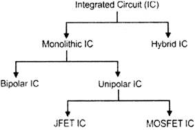
Simple circuits using semiconductor devices known as Integra circuit. The conventional method of making circuits is to choose components like diodes, transistor, R, L, C etc., and connect them by soldering wires in the desired manner. In spite of the miniaturization introduced by the discovery transistors, such circuits were still bulky. Apart from this. A circuits were less reliable and less shock proof.
The concept of fabricating an entire circuit (consisting of many passive components like R and C and active devices like du and transistor) on a small single block (or chip) of semiconductor has revolutionized the electronics technology Such a circuit is known as Integrated Circuit (1C), the most widely used technology is the Monolithic Integrated Circuit.
The word monolithic is a combination of two greek words, mono means single and lithic means stone.
Integrated circuit can be classified as shown in figure:
This, in effect, means that the entire circuit is formed on a single silicon crystal or chip. The chip dimensions are as small as 1m\[\times \]1mm or it could even be smaller. Figure shows a chip in protective plastic package, partly removed to reveal connections coming out from the 'chip' to the pins that enable to make external connections.
Depending on nature of input signals, IC's can be grouped in two categories:
(a) Linear or analogue IC's (b) Digital ICs.
The linear IC's process analogue signals which change smoothly and continuously over a range of values between a maximum and a minimum. The output is more or less directly proportional to the input, i.e., it varies linearly with the input. One of the most useful linear TC's is the operational amplifier.
The digital IC's process signals that have only two values 0 & 1. they contain circuits such as logic gates. Depending upon level of integration (i.e., the number of circuit components or logic gate), the ICs are termed as:
Small Scale Integration, SSI (logic gates < 10);
Medium Scale Integration, MSI (logic gates < 100);
Large Scale Integration, LSI (logic gates < 1000);
Very Large Scale Integration, VLSI (logic gates > 1000).
This technology of fabrication is very involved but large scale industrial production has made them very inexpensive.
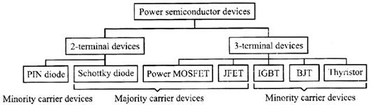
SEMICONDUCTOR POWER DEVICES
Power devices are divided into terms of their number of terminals:
A second classification has to do with the type of charge carriers they use:
MOSFET, JFET) - use only one type of charge carriers (i.e. either electrons or holes)
IGBT) - use both charge carriers (i.e. electrons and holes).
A third classification is based on the degree of controllability: uncontrollable switches (diodes), semi-controllable switches (thyristors); and fully-controllable switches (BJT, MOSFET, JFET, IGBT, GTO, MCT)
POWER SEMICONDUCTORS
(1) Power Semiconductor Diodes
It is a two-terminal, two-layer, one p-n junction, uncontrolled semiconductor device whose two terminals are anode, cathode and the symbol of diode as shown in the figure below.
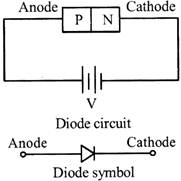
When the anode terminal is positive with respect to the cathode, the diode is said to be forward biased whereas when the cathode is positive with respect to the anode, it is said to be reverse biased.
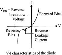
In forward bias condition, diode current rises rapidly after attaining a certain voltage which is known as the threshold voltage.
Under the reverse bias condition, due to minority carriers, a very small current flows through the diode known as leakage current.
If the applied reverse voltage increases, at a certain value breakdown voltage), the reverse bias junction will break down and high current starts conducting through the diode in the reverse direction.
Reverse recovery time is that interval in which reverse current flows through the thyristor during turn offs witching.
(2) Power Semiconductor Transistors
Power diodes are uncontrolled devices while the power transistors posses controlled characteristics. Power transistors are of three types.
(i) Bipolar Junction Transistors (BJT)
It is a three-terminal, three-layer, two–pn junction controlled device whose terminals are collector, base and emitter. Bipolar junction transistor is a current controlled device. A BJT continues to stay in the ON state till a current signal is given to its base. Once, the current signal is removed from the base, transistor is turned off.
When p-region is in between two n-regions, it is an npn transistor and when n-region is in between two p-regions, it is a pnp transistor as shown in the figure given below.
The symbols of both types of transistors are shown in the figure where the arrow indicates the direction off tow 01 emitter current.
(ii) MOSFET’S
(MOSFET) is a unipolar and voltage controlled device.
Static Characteristics of MOSFET
One of the important features of the power MOSFET is the very high impedance which simplifies the gate derive circuitry and reduces cost. It is a voltage controlled device with gate current flow during operation.
Working Principle of MOSFET
The working principle of MOSFET depends up on the MOS capacitor. The semiconductor surface at below the oxide layer and between the drain and source terminal can be inverted from p-type to n-type by applying a positive or negative gate voltages respectively. When we apply positive gate voltage the holes present beneath the oxide layer experience repulsive force and the holes are pushed downward with the substrate. The depletion region is populated by the bound negative charges, which are associated with the acceptor atoms. The positive voltage also attracts electrons from the n+ source and drain regions in to the channel. The electron reach channel is formed. Now, if a voltage is applied between the source and the drain, current flows freely between the source and drain gate voltage controls the electrons concentration the channel. Instead of positive if apply negative voltage a hole channel will be formed beneath the oxide layer. Now, the controlling of source to gate voltage is responsible for the conduction of current between source and the drain. If the gate voltage exceeds a given value called the three voltage only then the conduction begins
The current equation of MOSFET in triode region is —
\[{{I}_{d}}={{u}_{n}}{{C}_{ox}}\,\,\frac{W}{2}\,\,\left[ \left( {{V}_{GS}}-{{V}_{TH}} \right)\,\,{{V}_{DS}}-\frac{1}{2}\,\,V_{DS}^{2} \right]\]
Where, \[{{u}_{n}}\]= Mobility of the electrons
\[{{C}_{ox}}\]Capacitance of the oxide layer
W = Width of the gate area
L== Length of the channel
\[{{V}_{GS}}\]= Gate to Source voltage
\[{{V}_{TH}}\]= Threshold voltage
\[{{V}_{DS}}\]= Drain to Source voltage.
Comparison of MOSFET with BJT
MOSFETs are for high power functions.
(iii) IGBTs (Insulated Gate Bipolar Transistor)
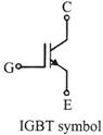
Static Characteristics of IGBT The circuit diagram, static V-I characteristics, and transfer characteristics of an IGBT are shew in figure below. The output \[V-I\]characteristics of an n-channel
IGBT show the plot of the collector current versus the gal emitter voltage. In the forward direction, the output characteristics are similar to those of the BJT. The only different is that the controlling parameter is the gate-emitter voltage.
The transfer characteristic is a plot of output collector current versus input gate-emitter voltage\[{{V}_{GE}}\].This characteristic identical to that of the power MOSFET and when the gate-emit) voltage\[{{V}_{GE}}\]is less than the threshold voltage\[{{V}_{GE}}\]device in the OFF-state. Thus, the transconductance of an IGBT defined as the ratio of the collector current to the gate-emitter voltage, i.e.
![]()
THYRISTORS
Thyristor is a four layer, three terminal, three junction controlled semiconductor device whose terminals are Anode, Cathode and Gate.
The schematic diagram and the symbols are shown in the figure below.
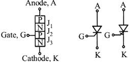
Schematic diagram Symbol of Thyristor
Thyristor Operation:
The whole operation of thyristor is divided in three modes:
Thus, junctions J 1 and J 3 are forward biased and junction J 2 is reverse biased. If forward voltage further increases, avalanche breakdown of junction J 2 occurs and the current starts conducting through the thyristor.
Due to this gate current, depletion layer of junction J 2 breaks at a much lower forward voltage and current begins to conduct through thyristor.
J1 and junction J3 are reverse biased and only junction J2 is forward biased.
Thus, no current flows through thyristor and only a small reverse current flows and that too because of minority carriers. If the magnitude of reverse voltage further increases, and reaches the level of breakdown, thyristor starts conducting in reverse direction.


You need to login to perform this action.
You will be redirected in
3 sec

