-
question_answer1)
When NPN transistor is used as an amplifier [AIEEE 2004]
A)
Electrons move from base to collector done
clear
B)
Holes move from emitter to base done
clear
C)
Electrons move from collector to base done
clear
D)
Holes move from base to emitter done
clear
View Solution play_arrow
-
question_answer2)
The phase difference between input and output voltages of a CE circuit is [MP PET 2004]
A)
0o done
clear
B)
90o done
clear
C)
180o done
clear
D)
270o done
clear
View Solution play_arrow
-
question_answer3)
An oscillator is nothing but an amplifier with [MP PET 2004]
A)
Positive feed back done
clear
B)
Large gain done
clear
C)
No feedback done
clear
D)
Negative feedback done
clear
View Solution play_arrow
-
question_answer4)
The emitter-base junction of a transistor is ?? biased while the collector-base junction is ??. biased [KCET 2004]
A)
Reverse, forward done
clear
B)
Reverse, reverse done
clear
C)
Forward, forward done
clear
D)
Forward, reverse done
clear
View Solution play_arrow
-
question_answer5)
In an NPN transistor the collector current is 24 mA. If 80% of electrons reach collector its base current in mA is [Kerala PMT 2004]
A)
36 done
clear
B)
26 done
clear
C)
16 done
clear
D)
6 done
clear
View Solution play_arrow
-
question_answer6)
A NPN transistor conducts when [CPMT 2003]
A)
Both collector and emitter are positive with respect to the base done
clear
B)
Collector is positive and emitter is negative with respect to the base done
clear
C)
Collector is positive and emitter is at same potential as the base done
clear
D)
Both collector and emitter are negative with respect to the base done
clear
View Solution play_arrow
-
question_answer7)
In the case of constants a and b of a transistor [CET 2003]
A)
a = b done
clear
B)
b < 1 a > 1 done
clear
C)
ab = 1 done
clear
D)
b > 1 a < 1 done
clear
View Solution play_arrow
-
question_answer8)
Which of the following is true [DPMT 2002]
A)
Common base transistor is commonly used because current gain is maximum done
clear
B)
Common emitter is commonly used because current gain is maximum done
clear
C)
Common collector is commonly used because current gain is maximum done
clear
D)
Common emitter is the least used transistor done
clear
View Solution play_arrow
-
question_answer9)
If a = 0.98 and current through emitter ie = 20 mA, the value of b is [DPMT 2002]
A)
4.9 done
clear
B)
49 done
clear
C)
96 done
clear
D)
9.6 done
clear
View Solution play_arrow
-
question_answer10)
For a common base configuration of PNP transistor \[\frac{{{l}_{C}}}{{{l}_{E}}}=0.98\] then maximum current gain in common emitter configuration will be [CBSE PMT 2002]
A)
12 done
clear
B)
24 done
clear
C)
6 done
clear
D)
5 done
clear
View Solution play_arrow
-
question_answer11)
In a PNP transistor working as a common-base amplifier, current gain is 0.96 and emitter current is 7.2 mA. The base current is [AFMC 2002; Pb. PET 2002]
A)
0.4 mA done
clear
B)
0.2 mA done
clear
C)
0.29 mA done
clear
D)
0.35 mA done
clear
View Solution play_arrow
-
question_answer12)
If \[{{l}_{1}},\,{{l}_{2}},\,{{l}_{3}}\] are the lengths of the emitter, base and collector of a transistor then [KCET 2002]
A)
\[{{l}_{1}}={{l}_{2}}={{l}_{3}}\] done
clear
B)
\[{{l}_{3}}<{{l}_{2}}>{{l}_{1}}\] done
clear
C)
\[{{l}_{3}}<{{l}_{1}}<{{l}_{2}}\] done
clear
D)
\[{{l}_{3}}>{{l}_{1}}>{{l}_{2}}\] done
clear
View Solution play_arrow
-
question_answer13)
In an NPN transistor circuit, the collector current is 10 mA. If 90% of the electrons emitted reach the collector, the emitter current (iE) and base current (iB) are given by [KCET 2001]
A)
iE = ? 1 mA, iB = 9 mA done
clear
B)
iE = 9 mA, iB = ? 1 mA done
clear
C)
iE = 1 mA, iB = 11 mA done
clear
D)
iE = 11 mA, iB = 1 mA done
clear
View Solution play_arrow
-
question_answer14)
In a common emitter transistor, the current gain is 80. What is the change in collector current, when the change in base current is 250 mA [CBSE PMT 2000]
A)
80 ´ 250 mA done
clear
B)
(250 ? 80) mA done
clear
C)
(250 + 80) mA done
clear
D)
250/80 mA done
clear
View Solution play_arrow
-
question_answer15)
Least doped region in a transistor [KCET 2000]
A)
Either emitter or collector done
clear
B)
Base done
clear
C)
Emitter done
clear
D)
Collector done
clear
View Solution play_arrow
-
question_answer16)
The transistors provide good power amplification when they are used in [AMU 1999]
A)
Common collector configuration done
clear
B)
Common emitter configuration done
clear
C)
Common base configuration done
clear
D)
None of these done
clear
View Solution play_arrow
-
question_answer17)
The transfer ratio of a transistor is 50. The input resistance of the transistor when used in the common-emitter configuration is 1 KW. The peak value for an A.C input voltage of 0.01 V peak is [CBSE PMT 1998]
A)
100 mA done
clear
B)
0.01 mA done
clear
C)
0.25 mA done
clear
D)
500 mA done
clear
View Solution play_arrow
-
question_answer18)
For a transistor the parameter b = 99. The value of the parameter a is [Pb CET 1998]
A)
0.9 done
clear
B)
0.99 done
clear
C)
1 done
clear
D)
9 done
clear
View Solution play_arrow
-
question_answer19)
A transistor is used in common emitter mode as an amplifier. Then [IIT-JEE 1998]
A)
The base-emitter junction is forward biased done
clear
B)
The base-emitter junction is reverse biased done
clear
C)
The input signal is connected in series with the voltage applied to the base-emitter junction done
clear
D)
The input signal is connected in series with the voltage applied to bias the base collector junction done
clear
View Solution play_arrow
-
question_answer20)
In a PNP transistor the base is the N-region. Its width relative to the P-region is [DCE 1997]
A)
Smaller done
clear
B)
Larger done
clear
C)
Same done
clear
D)
Not related done
clear
View Solution play_arrow
-
question_answer21)
A common emitter amplifier is designed with NPN transistor (a = 0.99). The input impedance is 1 KW and load is 10 KW. The voltage gain will be [CPMT 1996]
A)
9.9 done
clear
B)
99 done
clear
C)
990 done
clear
D)
9900 done
clear
View Solution play_arrow
-
question_answer22)
The symbol given in figure represents [AMU 1995, 96]
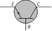
A)
NPN transistor done
clear
B)
PNP transistor done
clear
C)
Forward biased PN junction diode done
clear
D)
Reverse biased NP junction diode done
clear
View Solution play_arrow
-
question_answer23)
The most commonly used material for making transistor is [MNR 1995]
A)
Copper done
clear
B)
Silicon done
clear
C)
Ebonite done
clear
D)
Silver done
clear
View Solution play_arrow
-
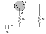
question_answer24)
An NPN-transistor circuit is arranged as shown in figure. It is [BHU 1994]
A)
A common base amplifier circuit done
clear
B)
A common emitter amplifier circuit done
clear
C)
A common collector amplifier circuit done
clear
D)
Neither of the above done
clear
View Solution play_arrow
-
question_answer25)
The part of a transistor which is heavily doped to produce a large number of majority carriers, is [CBSE PMT 1993]
A)
Base done
clear
B)
Emitter done
clear
C)
Collector done
clear
D)
None of these done
clear
View Solution play_arrow
-
question_answer26)
For a transistor, the current amplification factor is 0.8. The transistor is connected in common emitter configuration. The change in the collector current when the base current changes by 6 mA is [Haryana CET 1991]
A)
6 mA done
clear
B)
4.8 mA done
clear
C)
24 mA done
clear
D)
8 mA done
clear
View Solution play_arrow
-
question_answer27)
In a common base amplifier circuit, calculate the change in base current if that in the emitter current is 2 mA and a = 0.98 [BHU 1995]
A)
0.04 mA done
clear
B)
1.96 mA done
clear
C)
0.98 mA done
clear
D)
2 mA done
clear
View Solution play_arrow
-
question_answer28)
In case of NPN-transistors the collector current is always less than the emitter current because [AIIMS 1983]
A)
Collector side is reverse biased and emitter side is forward biased done
clear
B)
After electrons are lost in the base and only remaining ones reach the collector done
clear
C)
Collector side is forward biased and emitter side is reverse biased done
clear
D)
Collector being reverse biased attracts less electrons done
clear
View Solution play_arrow
-
question_answer29)
In a transistor circuit shown here the base current is 35 mA. The value of the resistor Rb is
A)
123.5 kW done
clear
B)
257 kW done
clear
C)
380.05 kW done
clear
D)
None of these done
clear
View Solution play_arrow
-
question_answer30)
In a transistor, a change of 8.0 mA in the emitter current produces a change of 7.8 mA in the collector current. What change in the base current is necessary to produce the same change in the collector current
A)
50 mA done
clear
B)
100 mA done
clear
C)
150 mA done
clear
D)
200 mA done
clear
View Solution play_arrow
-
question_answer31)
In a transistor configuration b-parameter is [Orissa PMT 2004]
A)
\[\frac{{{l}_{b}}}{{{l}_{c}}}\] done
clear
B)
\[\frac{{{l}_{c}}}{{{l}_{b}}}\] done
clear
C)
\[\frac{{{l}_{c}}}{{{l}_{a}}}\] done
clear
D)
\[\frac{{{l}_{a}}}{{{l}_{c}}}\] done
clear
View Solution play_arrow
-
question_answer32)
Which of these is unipolar transistor [Pb PMT 2004]
A)
Point contact transistor done
clear
B)
Field effect transistor done
clear
C)
PNP transistor done
clear
D)
None of these done
clear
View Solution play_arrow
-
question_answer33)
For a transistor, in a common emitter arrangement, the alternating current gain b is given by [DPMT 2004]
A)
\[\beta ={{\left( \frac{\Delta {{I}_{C}}}{\Delta {{I}_{B}}} \right)}_{{{V}_{C}}}}\] done
clear
B)
\[\beta ={{\left( \frac{\Delta {{I}_{B}}}{\Delta {{I}_{C}}} \right)}_{{{V}_{C}}}}\] done
clear
C)
\[\beta ={{\left( \frac{\Delta {{I}_{C}}}{\Delta {{I}_{E}}} \right)}_{{{V}_{C}}}}\] done
clear
D)
\[\beta ={{\left( \frac{\Delta {{I}_{E}}}{\Delta {{I}_{C}}} \right)}_{{{V}_{C}}}}\] done
clear
View Solution play_arrow
-
question_answer34)
The relation between a and b parameters of current gains for a transistors is given by [Pb. PET 2000]
A)
\[\alpha =\frac{\beta }{1-\beta }\] done
clear
B)
\[\alpha =\frac{\beta }{1+\beta }\] done
clear
C)
\[\alpha =\frac{1-\beta }{\beta }\] done
clear
D)
\[\alpha =\frac{1+\beta }{\beta }\] done
clear
View Solution play_arrow
-
question_answer35)
When NPN transistor is used as an amplifier [DCE 2002]
A)
Electrons move from base to emitter done
clear
B)
Electrons move from emitter to base done
clear
C)
Electrons moves from base to emitter done
clear
D)
Holes moves from base to emitter done
clear
View Solution play_arrow
-
question_answer36)
In the CB mode of a transistor, when the collector voltage is changed by 0.5 volt. The collector current changes by 0.05 mA. The output resistance will be [Pb. PMT 2003]
A)
10 kW done
clear
B)
20 kW done
clear
C)
5 kW done
clear
D)
2.5 kW done
clear
View Solution play_arrow
-
question_answer37)
Which of the following is used to produce radio waves of constant amplitude [DCE 2004]
A)
Oscillator done
clear
B)
FET done
clear
C)
Rectifier done
clear
D)
Amplifier done
clear
View Solution play_arrow
-
question_answer38)
While a collector to emitter voltage is constant in a transistor, the collector current changes by 8.2 mA when the emitter current changes by 8.3 mA. The value of forward current ratio hfe is [KCET 2002]
A)
82 done
clear
B)
83 done
clear
C)
8.2 done
clear
D)
8.3 done
clear
View Solution play_arrow
-
question_answer39)
Consider an NPN transistor amplifier in common-emitter configuration. The current gain of the transistor is 100. If the collector current changes by 1 mA, what will be the change in emitter current [AIIMS 2005]
A)
1.1 mA done
clear
B)
1.01 mA done
clear
C)
0.01 mA done
clear
D)
10 mA done
clear
View Solution play_arrow
-
question_answer40)
In a common base amplifier the phase difference between the input signal voltage and the output voltage is [CBSE PMT 1990; AIEEE 2005]
A)
0 done
clear
B)
\[\pi /4\] done
clear
C)
\[\pi /2\] done
clear
D)
\[\pi \] done
clear
View Solution play_arrow
-
question_answer41)
In NPN transistor the collector current is 10 mA. If 90% of electrons emitted reach the collector, then [Kerala PMT 2005]
A)
Emitter current will be 9 mA done
clear
B)
Emitter current will be 11.1 mA done
clear
C)
Base current will be 0.1 mA done
clear
D)
Base current will be 0.01 mA done
clear
View Solution play_arrow
-
question_answer42)
NPN transistor are preferred to PNP transistor because they have [J & K CET 2005]
A)
Low cost done
clear
B)
Low dissipation energy done
clear
C)
Capability of handing large power done
clear
D)
Electrons having high mobility than holes done
clear
View Solution play_arrow
-
question_answer43)
In a transistor in CE configuration, the ratio of power gain to voltage gain is [J & K CET 2005]
A)
a done
clear
B)
b / a done
clear
C)
ba done
clear
D)
b done
clear
View Solution play_arrow
-
question_answer44)
In the study of transistor as an amplifier, if \[\alpha ={{I}_{c}}/{{I}_{e}}\] and \[\beta ={{I}_{c}}/{{I}_{b}},\] where \[{{I}_{c}},{{I}_{b}}\] and Ie are the collector, base and emitter currents, then [CBSE PMT 2000; KCET 2000; Orissa JEE 2005]
A)
\[\beta =\frac{1-\alpha }{\alpha }\] done
clear
B)
\[\beta =\frac{\alpha }{1-\alpha }\] done
clear
C)
\[\beta =\frac{\alpha }{1+\alpha }\] done
clear
D)
\[\beta =\frac{1+\alpha }{\alpha }\] done
clear
View Solution play_arrow


