Analog and Digital Electronics
Category : Railways
Analog and Digital Electronics
ANALOG ELECTRONICS
PN JUNCTION DIODE
A diode is a two-terminal pn junction device.
The material so used in order to make this PN junction is either Germanium or Silicon.
The fig. snows the schematic symbol of a PN junction Diode:
According to the symbol, the arrow pointing towards the terminal is the Cathode and the other end is the Anode.
![]()
Fig.: PN Junction Diode
Modes of Operation
There are generally two types of modes of operation for diodes:
(i) Forward Bias: When an external voltage source is applied to one end of the junction in such a manner that it overcomes the potential barrier and permits current to flow, it is called Forward Biasing.
In case of a PN junction Diode, in order to operate the diode in the forward biasing mode, the p-type semiconductor (anode) is connected to the positive terminal, while the n-type semiconductor (cathode) is connected to the negative terminal of an external voltage source as shown in the fig.
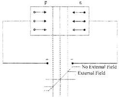
Fig.: Forward Biasing
(ii) Reverse Bias: This acts opposite to the forward biasing mode i.e. in this mode an external voltage source is connected in such a manner, that it will increase the potential barrier and resist the flow of current, m this mode the p-type semiconductor (anode) is connected to the negative terminal and the n-type semiconductor (cathode) is connected to the positive terminal as shown in fig.
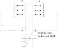
Fig.: Reverse Biasing
V-I Characteristics
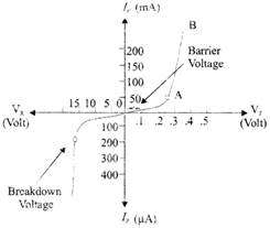
Fig.: V-I Characteristics
Effect of Temperature on Diode Characteristic
In the last section, we had discussed about diode current equation, in which it is clearly mentioned that diode current is a function of temperature and since the coefficient of temperature\[\left( {{V}_{T}} \right)\]is in the denominator of the power of the exponential term:
\[I={{I}_{0}}({{e}^{V/{{\eta }^{V}}T-1}})\]
therefore, with an increase in the temperature, the diode current exponentially decreases and vice versa. However, there is one more term mentioned in this equation, which is the saturation current\[({{I}_{0}})\], the variation for which is much greater than the exponential term.
ZENER DIODE
Zener Diode is a special purpose silicon PN junction diode which differs from other diodes in the sense that it operates in the reverse biased mode.
Zener diode is also known as a voltage regulator or voltage reference or breakdown diode. The Fig. shows the symbol for a zener diode:
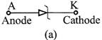
Fig.: Symbol of Zener Diode
The breakdown voltage of a Zener diode is carefully controlled by maintaining the doping level during manufacturing. So, if the doping level is high, then depletion layer is thin and breakdown occurs at a low reverse voltage. When reverse voltage is increased, a critical voltage called breakdown voltage is reached at which reverse current will sharply increase.
Zener Diode Applications
(i) As a voltage regulator
(ii) As a fixed reference voltage in biasing circuits
(iii) In clipper circuits.
BJT-BIPOLAR JUNCTION TRANSISTOR
Transistors are basic building blocks of electronics used for amplifiers and switching signals.
The basic definition of BJT is "It is a three terminal device whose output voltage/current or power is controlled by its input current."
It is a current-controlled current source device.
There are two types of transistors namely-
(i) \[n-p-n\] transistor
(ii) \[p-n-p\] transistor
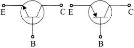
Fig. p-n-p transistor
In an n-p-n transistor, two n-type semiconductors are separated by a thin layer of a p-type semiconductor, while in a p-n-p transistor, two p-type semiconductors are separated by a thin layer of n-type semiconductor.
Modes of Operation
When the transistor is connected to the external voltage source, it is called biasing.
Active Mode: In this mode, suppose we are using an NPN transistor. As shown in fig. the base-emitter junction is forward biased and base-collector junction is reverse biased.
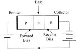
Fig.
Saturation Mode: In this mode, both the junctions (base-emitter and base -collector) are forward biased, due to which a large value of current is obtained. This mode is mainly used when the transistor is used in switching.
Cut-off Mode: In the cut-off mode, both the emitter -base junction as well as the collector-base junction are reverse biased and have zero current. For example, if the transistor is to be operated as an open switch, this mode can be used.
Current Gain
Current Gain is defined as "The ratio of change in collector current to the change in emitter current at constant collector base voltage.
\[\propto =\frac{\Delta {{I}_{C}}}{\Delta {{I}_{E}}}\,\,\,\,\,{{V}_{CB}}\text{Constant}\]
Collector current \[{{I}_{C}}=\frac{\propto }{1-\propto }{{I}_{B}}+\frac{{{I}_{CBO}}}{1-\propto }\]
Base amplification factor (\[\beta \]): It is defined as the ratio of change in collector current to the change in base current."
\[\beta =\frac{\Delta {{I}_{C}}}{\Delta {{I}_{B}}}\]
Collector Current \[{{I}_{C}}=\alpha {{I}_{B}}+\alpha {{I}_{C}}+{{I}_{CBO}}\]
Relation between \[\alpha \] and \[\beta \]
\[\left[ \beta =\frac{\alpha }{1-\alpha } \right]\]
Current Amplification Factor: \[\gamma =\frac{\Delta {{I}_{E}}}{\Delta {{I}_{B}}}\]
Relation Between\[\gamma \]and\[\alpha \]:\[=\frac{1}{1-\alpha }\]
Collector current: \[{{I}_{C}}=(\beta +1)\,\,{{I}_{B}}+(\beta +1)\,\,{{I}_{CBO}}\]
OSCILLATOR
An oscillator is a mechanical or electronic device that works on the principles of oscillation: aperiodic fluctuation between two things based on changes in energy. Computers, clocks, watches, radios, and metal detectors are among the many devices that use oscillator.
Practically, the oscillators are nothing but the amplifier circuits which are provided with a positive or regenerative feedback where in a part of the output signal is fed back to the input. Here the amplifier consists of an active amplifying element which can be a transistor or an Op-Amp and the back-fed in-phase signal 15 held responsible to keep-up (sustain) the oscillations by making- up for the losses in the circuit.
Oscillators can be classified into various types depending on the parameter considered viz.
Wave oscillators, Sweep Oscillators (which produce saw-tooth output waveform), etc.
Oscillators, etc.
Oscillators (which use a quartz crystal to result in a frequency stabilized output waveform), etc.
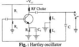
Types of Oscillators
Where, \[{{L}_{1}}\]is the inductance in Henry
\[{{C}_{1}}\]is the capacitance is Farad
f is the output frequency in Hertz
\[f=\frac{1}{2\pi \sqrt{{{L}_{T}}C}}\]
Where\[{{L}_{T}}\]\[=\]\[{{L}_{1}}+{{L}_{2}}+2M\]
The Hartley Oscillator consists of a parallel LC resonator tank circuit whose feedback is achieved by way of an inductive divider. Like most oscillator circuits, the Hartley oscillator exists in several forms, with the most common form being the transistor circuit.
The basic configuration of the Colpitts Oscillator resembles that of the Hartley Oscillator but the difference this time is that the centre tapping of the tank sub-circuit is now made at the junction of &"capacitive voltage divider" network instead of a tapped autotransformer type inductor as in the Hartley oscillator.
The frequency of oscillations for a Colpitts Oscillator is given as
\[{{f}_{r}}=\frac{1}{2\pi \sqrt{L{{C}_{T}}}},{{C}_{T}}={{C}_{1}}||{{C}_{2}}\]
\[f=\frac{1}{2\pi RC\sqrt{2N}}\]
\[f=\frac{K}{t}\]
Series resonant frequency \[{{f}_{s}}=\frac{1}{2\pi \sqrt{LC}}\]
Parallel Resonant Frequency \[{{f}_{p}}=\frac{1}{2\pi \sqrt{L{{C}_{T}}}}\]
Where \[{{C}_{T}}=\frac{C{{C}_{M}}}{C+{{C}_{m}}}\]
\[f=\frac{1}{2\pi \sqrt{{{R}_{1}}{{C}_{1}}{{R}_{2}}{{C}_{2}}}}\]
Or \[{{R}_{1}}={{R}_{2}}=R;\] \[C={{C}_{1}}={{C}_{2}}\]
\[f=\frac{1}{2\pi \sqrt{{{R}^{2}}{{C}^{2}}}}=\frac{1}{2\pi RC}\]
The Wien Bridge Oscillator is so called because the circuit is based on a frequency-selective form of the Wheatstone bridge circuit. The Wien Bridge oscillator is a two-stage
RC coupled amplifier circuit that has good stability at its resonant frequency, low distortion and is very easy to tune making it a popular circuit as an audio frequency oscillator but the phase shift of the output signal is considerably different from the previous phase shift RC Oscillator.
Field effect transistor
The concept of the field effect transistor is based around the concept that charge on a nearby object can attract charges within a semiconductor channel. It essentially operates using an electric field effect - hence the name.
The FET consists of a semiconductor channel with electrodes at either end referred to as the drain and the source.
A control electrode called the gate is placed in very close proximity to the channel so that its electric charge is able to affect the channel.
In this way, the gate of the FET controls the flow of carriers (electrons or holes) flowing from the source to drain. It does this by controlling the size and shape of the conductive channel.
The semiconductor channel where the current flow occurs may be either P-type or N-type. This gives rise to two types or categories of FET known as P-Channel and N-Channel FETs.
In addition to this, there are two further categories. Increasing the voltage on the gate can either deplete or enhance the number of charge carriers available in the channel. As a result there are enhancement mode FET and depletion mode FETs.
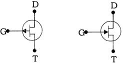
p channel JFET (i) n channel JFET (ii)
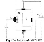
MOSFET: Metal Oxide Semiconductor Field Effect
Transistor.
MOSFET is somewhat similar to a JFET as it also has three terminals called the source, gate and the drain. Sometimes, MOSFET is also known as IGFET which stands for Insulated gate Field Effect Transistor because the gate of MOSFET is insulated from channel. There are further classifications of MOSFET given as-
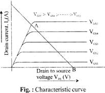
Drain characteristic of Depletion -Type MOSFET
The drain current characteristic curve is made between drain current along y-axis and drain to source voltage along x-axis.as shown in the fig.
\[{{I}_{D}}={{I}_{DSS}}\,\,{{\left[ 1-\frac{{{V}_{GS}}}{{{V}_{P}}} \right]}^{2}}\]
Introduction to the Amplifier
Amplifier is the generic term used to 'describe a circuit which increases its input signal, but not all amplifiers are the same as they are classified according to their circuit configurations and methods of operation.
In "Electronics", small signal amplifiers are commonly used devices as they have the ability to amplify a relatively small input signal, for example from a sensor such as a photo-device, into a much larger output signal to drive a relay, lamp or loudspeaker for example.
There are many forms of electronic circuits classed as amplifiers, from Operational Amplifiers and Small Signal Amplifiers up to
Large Signal and Power Amplifiers. The classification of an amplifier depends upon the size of the signal, large or small, its physical configuration and how it processes the input signal that is the relationship between input signal and current flowing in the load.
The type or classification of an Amplifier is given in the following table.
Classification of Amplifiers
Amplifier Gain
The introduction to the amplifier gain can be said to be the relationship that exists between the signal measured at the output with the signal measured at the input. There are three different kinds of amplifier gain which can be measured and these are: Voltage Gain (Av), Current Gain (Ai) and Power Gain (Ap) depending upon the quantity being measured with examples of these different types of gains are given below.
Voltage Amplifier Gain
Voltage Gain \[({{A}_{V}})=\frac{output\,\,Voltage}{Input\,\,Voltage}=\frac{V\,\,\,\,\,out}{V\,\,\,\,\,\,in}\]
Current Amplifier Gain
Current Gain \[({{A}_{i}})=\frac{output\,Current}{Input\,\,Current}=\frac{I\,\,out}{I\,\,\,in}\]
Power Amplifier Gain
Power Gain \[({{A}_{P}})={{A}_{v}}x\,\,{{A}_{i}}\]
IC-555 TIMER
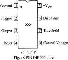
IC - 555 Timer as Astabel Multivibrator
Duty cycle. The duty-cycle is the ratio of time in the high state to the total period, T and is given by
Duty cycle\[=\frac{{{t}_{c}}}{T}=\frac{({{R}_{1}}+{{R}_{2}})}{({{R}_{1}}+2{{R}_{2}})}\]
DIGITAL ELECRONICS
NUMBER SYSTEM
Binary Number System
The number system with base for radix) two is known as the binary number system. Only two symbols are used to represent numbers in this system and these are 0 and 1, these are known as bits. It is a positional system, that is every position is assigned a specific weight left - most bit is known as Most Significant Bit (MSB) and the right - most bit is known as the Least Significant Bit (LSB)
|
Number system |
Base or radix (b) |
Symbol used (di or \[{{d}_{-f}}\]) |
Weight assigned to position |
example |
|
Binary |
2 |
0,1 |
\[{{2}^{-i}}\,\,\,\,\,\,{{2}^{-f}}\] |
1011.11 |
|
Octal |
8 |
0,1,2,3,4 |
\[{{8}^{-i}}\,\,\,\,\,\,\,{{8}^{-f}}\] |
3567.25 |
|
Decimal |
10 |
0,1,2,3,4,5 |
\[{{10}^{-i}}\,\,\,\,\,{{10}^{-f}}\] |
3974.57 |
|
Hexadecimal |
16 |
0,1,2,3,4,5,6,7,8 A,B,C,D,E,F |
\[{{16}^{-i}}\,\,\,\,\,\,{{16}^{-f}}\] |
3FA9.56 |
NUMBER CONVERSIONS
Binary-Decimal Conversion
Any binary number can be converted into its equivalent decimal number using the weights assigned to each bit position. Since only two digits are used, the weights are powers of 2. These weight are \[2{}^\circ \] (Units), \[{{2}^{1}}\] (twos), \[{{2}^{2}}\] (fours) \[{{2}^{3}}\] (eights) and \[{{2}^{4}}\] (sixteen). If longer binary number involved, the weights continue is ascending powers of 2.
The decimal equivalent of a binary number equals the sum of all binary number equal the sum of all binary digits multiplied by their weights.
Example 1: Find the decimal equivalent of binary number 11111.
Solution:
The equivalent decimal number is,
\[=1\times {{2}^{4}}+1\times {{2}^{3}}+1\times {{2}^{2}}+1\times {{2}^{1}}+1\times {{2}^{0}}\]
\[=16+8+4+2+1={{(31)}_{10}}\]
Decimal-to Binary Conversion
Any decimal number can be converted into its equivalent binary number. For integers, the conversion is obtained by continuous division by 2 and keeping track of the remainders, while for fractional parts, the conversion is effected by continuous multiplications by 2 and keeping track of the integers generated.
Example 2: Express the 25.5 decimal number in the binary form.
Solution:
Integer Part;
Thus,\[{{(25)}_{10}}={{(11001)}_{2}}\]
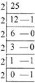
Read down to up
Fraction part
\[\begin{matrix}
0 & . & 5 \\
\times & {} & 2 \\
1 & . & 0 \\
\end{matrix}\]
i.e., \[{{0.5}_{10}}={{0.1}_{2}}\]
Therefore \[{{25.5}_{10}}={{11001.1}_{2}}\]
Decimal - Octal Conversion
This can be achieved by dividing the given decimal number repeatedly by 8, until a quotient of 0 is obtained.
Example 3: Convert con version \[{{(444.499)}_{10}}\]
Solution:
|
Division |
|
Generated Remainder |
|
444/8 |
|
|
|
55/8 |
\[\to \] |
4 |
|
6/8 |
\[\to \] |
7 |
|
0/8 |
\[\to \] |
6 |
On reading the remainders from bottom to top, the decimal
\[{{(444)}_{10}}\to {{(674)}_{8}}\]Now, fractional conversion
|
Multiplication |
Generated Integer |
|
\[0.499\times 8=3.992\] |
3 |
|
\[0.992\times 8=7.936\] |
7 |
|
\[0.936\times 8=7.488\] |
7 |
|
\[0.488\times 8=3.904\] |
3 |
The process gets terminated when significant digits are acquired. Thus, octal equivalent is\[{{(444.499)}_{10}}={{(674.3773)}_{8}}\]
Octal - Binary Conversion
It can be explained through the following example: To convert \[{{(377)}_{8}}\]into binary, replace each significant digit by its \[3-\]bit binary equivalent.
\[{{(377)}_{8}}=\begin{matrix}
3 & 7 & 7 & {} & {} \\
{} & {} & =011 & 111 & 111 \\
\end{matrix}\]
Thus, \[{{(377)}_{8}}={{(011111111)}_{2}}\]
Binary-Hexadecimal Conversion
\[e.g.,\,\,{{(10100110111110)}^{2}}\]
\[={{(0010100110111110)}^{2}}={{(2\,\,9\,\,B\,\,E)}_{16}}\times 1\]
Hexadecimal-Binary Conversion
It can be explained through an example. To convert \[{{(I\,\,D5)}_{16}}\]into binary, replace each significant digit by its 4-bit binary equivalent.
\[\begin{matrix}
{{(1D5)}_{16}} & = & 1 & D & 5 \\
{} & = & 0001 & 1101 & 0101 \\
\end{matrix}\]
Thus,\[{{(ID5)}_{16}}\] \[={{(000111010101)}_{2}}\]
SIGNED NUMBERS
Representation for signed binary numbers:
(i) Signed and Magnitude: m this representation, MSB is used to represent sign (0 for positive and 1 for negative) and remaining bits are used to represent magnitude of the number, e.g., binary \[6-bit\]number 011010 represent positive number and its value is 26, whereas111010 represents a negative number written as\[-26.\]
(ii) One's complement notation: In a binary number, if we replace each 0 by 1.and each 1 by 0, we obtain another binary number which is one's complement of the first binary number, e.g., while (0111); represents \[{{(+7)}_{10,}}{{(1000)}_{2}}\]
In general, maximum positive and negative number that can be represented by \[\left( {{2}^{n-1}}-1 \right)\]and\[\left( {{2}^{n-1}}-1 \right)\] respectively.
(iii) Two's complement notation: By adding 1 to the one's complement of a binary numbers we get two's complement of that binary number. e.g., 0101 represents +5, where as its complement, 1011 (Is complement+1) represents\[-5.\]
DIGITAL LOGICAL GATES
OR Gate: Its symbol is given in the fig. (a) & its truth table is (a)
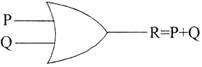
Fig (a): OR Gate
Table (a)
|
Inputs |
Output R=P+Q |
|
|
P |
Q |
|
|
0 |
0 |
0 |
|
0 |
1 |
1 |
|
1 |
0 |
1 |
|
1 |
1 |
1 |
AND Gate: Its symbol is given in the fig. (b) &. its truth table is (b)
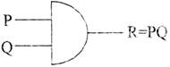
Fig.(b) : AND Gate
Table (b)
|
Inputs |
Output R=P.Q |
|
|
P |
Q |
|
|
0 |
0 |
0 |
|
0 |
1 |
0 |
|
1 |
0 |
0 |
|
1 |
1 |
1 |
NOT Gate (Inverter): Its symbol is given in the fig. (c) & its truth table is (c)
![]()
Fig. (c): NOT Gate
Table (c)
|
Input P |
Output R |
|
0 |
1 |
|
1 |
0 |
NAND Gate: Its symbol is given in in the fig. (d) & its truth table is (d)
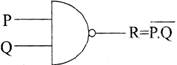
Fig. (d): NAND Gate
Table (d)
|
Inputs |
Output R |
|
|
P |
Q |
|
|
0 |
0 |
1 |
|
0 |
1 |
1 |
|
1 |
0 |
1 |
|
1 |
1 |
0 |
NOR Gate: Its symbol is given in the fig. (e) & its truth table is (e)
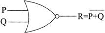
Fig (e): NOR Gate
Table (e)
|
Inputs |
Output R |
|
|
P |
Q |
|
|
0 |
0 |
1 |
|
0 |
1 |
0 |
|
1 |
0 |
0 |
|
1 |
1 |
0 |
BOOLEAN ALGEBRA
Some more Boolean laws:
(1) P+0=P (2) P+1=1
(3) P+P=P (4) P+P=1
(5) P.1=P (6) P.0=0
(7) P.P=P (8) P.P=0
(9) \[\overline{P}=\overline{P}\] (10) \[\overline{\overline{P}}=P\]
Demorgan's Theorems:
Half Adder
In .order to solve arithmetic operations, this type of devices are introduced. Half Adder is used for the addition of two bits. Half adder generates two outputs as SUM and CARRY. The logical diagram along with truth table 5 is depicted.
\[Sum=A\oplus B\]
\[Carry=A.B\]
Truth Table
|
A |
B |
SUM(S) |
CARRY(C) |
|
0 |
0 |
0 |
0 |
|
0 |
1 |
1 |
0 |
|
1 |
0 |
1 |
0 |
|
1 |
1 |
0 |
1 |
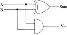
Fig.: Half adder
FULL ADDER
A full adder is a device capable of adding three bits as show figure. Full Adder generates two outputs same as half adder
Sum\[=A\oplus B\oplus C\]
Carry =AB+BC+CA
Truth Table
Table
|
A |
B |
Carry-in \[({{C}_{in}})\] |
SUM(S) |
CARRY(C) |
|
0 |
0 |
0 |
0 |
0 |
|
0 |
0 |
1 |
1 |
0 |
|
0 |
1 |
0 |
1 |
0 |
|
0 |
1 |
1 |
0 |
1 |
|
1 |
0 |
0 |
1 |
0 |
|
1 |
0 |
1 |
0 |
1 |
|
1 |
1 |
0 |
0 |
1 |
|
1 |
1 |
1 |
1 |
1 |
CANONICAL NORMAL FORMS
Sum of Products (SOP) Method
It is an expression which denotes the logical sum of two or more logical product terms. It is basically an OR operation of AND operated variables such as
\[Y=PQ+QR+PR,\] or \[Y=PQ+\overline{P}R+QR\]
Product of Sums (POS) Method
It is an expression which denotes the logical product of two or more logical sum terms. It is basically an AND operation of OR operated variables such as
\[Y=(P+Q)\,\,(Q+R)\,\,(R+\overline{P}),\,\,or\]\[Y=(P+Q+R)\,\,(P+\overline{R})\]
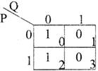
Karnaugh Map (K-Map) Simplification
It is a technique for simplifying & manipulating switching expressions. It is a modified form of a truth table where information contained either in truth table or in POS or in SOP form is represented on the K-map.
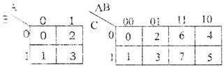
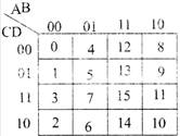
Fig.: Two Variable Fig.: Three Variable Fig.: Four Variable
Basic Rules
The decimal codes are given inside each cell at the bottom right corner (which is basically a combination of corresponding variables)
Don’t Care Conditions
MULTIPLEXER
A Multiplexer is a Data selector, which gets several input signals to the single output. The method of selecting one of the several inputs is controlled by Control lines. We can define multiplexer as "a device consists of n-input line and having a single output line to process". Generally multiplexers are used in parallel - to serial conversion of data because it is used for routing several signals to the same destination, for example bus, synchronous transmission etc. In other words, we can say that a multiplexer is a digitally controlled multi-position switch. The fig. shows the block diagram of a multiplexer:
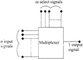
Fig.: Block diagram of multiplexer
Application of MUX:
DEMULTIPLEXER
The working of a demultiplexer is exactly opposite to that of a multiplexer. Demultiplexer receives information from a single line and transmits it to several lines. That is why demultiplexer is used in serial-to-parallel conversion and Data Distributors. The fig. shows the block diagram of a Demultiplexer with one input signal, m select signals and n output signals.
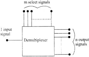
Fig.: Block diagram of de-multiplexer
FLIP FLOPS
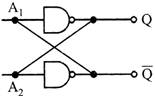
Fig. (a): Basic Memory Cell
(a) S-R (Set - Reset) Flip-Hops
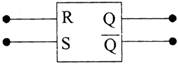
Fig. (b) : Block diagram
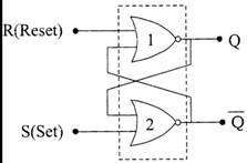
Fig. (c): NOR based S-R flip-flop
(b) Clocked S-R Flip-flop
The clocked SR flip-flop shown in fig. (d) consists of a basic NOR flip-flop and two AND gates. The outputs of the two AND gates remain at 0 as long as the clock pulse (or CP) is 0, regardless of the S and R input values. When the clock (clock pulse)
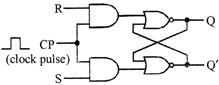
Fig. (d): Clocked \[SR\]Flip-flop
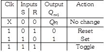
pulse goes to 1, information from the S and R inputs passes through to the basic flip-flop. With both S=1 and R=1, the occurrence of a clock pulse causes both outputs to momentarily go to 0. When the pulse is removed, the state of the flip-flop is indeterminate, i.e., either state may result, depending on whether the set or reset input of the flip-flop remains a 1 longer than the transition to 0 at the end of the pulse. \[{{Q}_{n+1}}={{S}_{n}}+{{R}_{n}}'{{Q}_{n}}\]
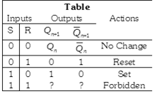
Table: \[SR\]Flip-flop Truth Table

The disadvantage of S-R flip-flop is for S=1, R=1 output cannot be determined. This can be eliminated in \[JK\]flip - flop.\[SR\] flip flop can be converted to \[JK\]flip - flop by using the two equation S=JQ' and R=KQ.
(c) J - K Flip-flops:
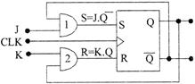
Fig. (e): \[JK\]flip - flop using \[S-R\]flip-flop
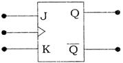
Fig. (f): Graphic symbol of J-K flip flop
Table
The Master-Slave JK Flip - flop
The Master-Slave Flip-Flop is basically two gated SR flip - flops connected together in a series configuration with the slave having an inverted clock pulse. The outputs from Q and Q from the "Slave" flip-flop are fed back to the inputs of the "Master" with the outputs of the "Master" flip-flop being connected to the two inputs of the "Slave" flip-flop.
This feedback configuration from the slave's output to the master's input gives the characteristic toggle of the JK flip- flop as shown in fig. (g).The input signals J and K are connected to the gated "master" SR flip-flop which "locks" the input condition while the clock (Clk) input is "HIGH" at logic level "I". As the clock input of the "slave" flip-flop is the inverse (complement) of the "master" clock input, the "slave" SR flip - flop does not toggle. The outputs from the "master" flip - flop are only "seen" by the gated "slave" flip - flop when the clock input goes "LOW" to logic level "O".
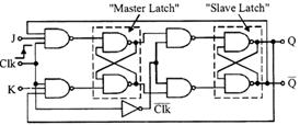
Fig. (g): The Master-Slave JK Flip-Flop
When the clock is "LOW", the outputs from the "master" flip-flop are latched and any additional changes to its inputs are ignored. The gated "slave" flip-flop now responds to the state of its inputs passed over by the "master" section. Then on the "Low-to-High" transition of the clock pulse the inputs of the "master" flip-flop are fed through to the gated inputs of the "slave" flip-flop and on the "High-to-Low" transition the same inputs are reflected on the output of the "slave" making this type of flip-flop edge or pulse- triggered.
Then, the circuit accepts input data when the clock signal is "HIGH", and passes the data to the output on the falling- edge of the clock signal. In other words, the Master-Slave
JK Flip-Hop is a "Synchronous" device as it only passes data with the timing of the clock signal.
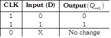
(d) D Flip-Hops:
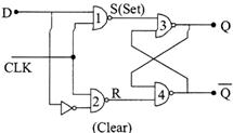
Fig. (h): D-flip-flop Using NAND gates
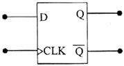
Fig. (i): Logic symbol
Table
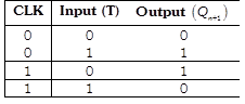
(e) T Flip - flops
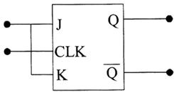
Fig. (j): T flip flop using a J-K-flip flop
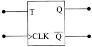
Fig. (k): Block diagram of T flip flop
Table
COUNTERS
A counter is a special kind of register, designed to count the number of clock pulses arriving at its input. It is one of the most useful subsystem in a digital systems. The input to this counter is a rectangular waveform called clock. Each time the clock signal changes state from low to high, the counter will add one (1) to the number stored in its Hip flop. This means the counter will count the number of clock transitions from low to high.
A clock having a small circle (bubble) in the input side would count clock transitions form high to low. Since clock pulses occur at known intervals, the counter can be used as an instrument for measuring time and therefore frequency. There are basically two different types of counters Synchronous and Asynchronous.
(a) Synchronous counters: The ripple counter is the simplest of all kinds of counters. But the problem with it is its delay time. In a ripple counter each flip - flop has a delay time and these delay times are additive. Therefore the total "settling" time for the counter is equal to the delay time multiplied by total number of flip - flops. This problem can be overcome by the use of a synchronous or parallel counter. Here every flip-flop is triggered in synchronism with the clock.
(i) Ring Counter: A ring counter is a shift-left register because the bits are shifted left one position per positive clock edge. But the final output is feedback to the Do input. This kind of action is known as "rotate left" the bits are shifted left and fed back to the input.
(ii) Decode counter (Mode - 10 counter): A counter with 10 distinct states is known as a decade counter. This counter counts 10 sequences and reset on 10th clock pulse. That is, the circuit count from 0000 to 1001 and on the tenth clock pulse, it generates its own clear signal and count jump back to 0000.
(b) Asynchronous counter (ripple counter): When the output of a flip-flop is used as the clock input for the next flip-flop we call the counter as a ripple counter or asynchronous counter. The triggers move through the flip-flops like ripple in water — because of this, the overall settling time is the sum of the individual delays.
ANALOG TO DIGITAL CONVERTER (A/D)
Quantizing: Breaking down of analog values into finite states. Encoding: Assigning a digital number to each state & matching it to the input signal.
Either by increasing the resolution which improves the accuracy in measuring the amplitude of the analog signal. By increasing the sampling rate which increases the maximum frequency that can be measured.
DIGITAL TO ANALOG CONVERTER
Sampling: Measurement at regular intervals of the amplitude of varying waveform.
Quantizing: Breaking down of analog value into finite states.
It is used for the generation of audio signals.
DECODER
\[\Rightarrow \]Decoder is combinational ckt which have many i/p and many o/p.
\[\Rightarrow \]It is used to convert binary data to other code (binary to ****)
BCD to Decimal (4\[\times \]10)
Binary to Hexadecimal
BCD to seven segment
\[\Rightarrow \]2 to 4 decoder is minimum possible decoder.
2 \[\times \] 4 Decoder:-
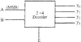
Fig. (a): DECODER
THE SHIFT REGISTER
The Shift Register is another type of sequential logic circuit that is used for the storage or transfer of data in the form of binary I numbers and then "shifts" the data out once every clock cycle. hence the name "shift register". It basically consists of several single bit "D-Type Data Latches", one for each bit (0 or connected together in a serial or daisy-chain arrangement so that the output from one data latch becomes the input of the next latch and so on.
Generally, shift registers operate in one of four different modes with the basic movement of data through a shift register being:


You need to login to perform this action.
You will be redirected in
3 sec

