Biasing
Category : JEE Main & Advanced
It means the way of connecting emf source to P-N junction diode. It is of following two types
(1) Forward biasing : Positive terminal of the battery is connected to the P-crystal and negative terminal of the battery is connected to N-crystal
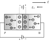
(i) In forward biasing width of depletion layer decreases
(ii) In forward biasing resistance offered \[{{R}_{\text{Forward}}}\approx 10\Omega -25\Omega \]
(iii) Forward bias opposes the potential barrier and for \[V>{{V}_{B}}\] a forward current is set up across the junction.
(iv) The current is given by \[i={{i}_{s}}({{e}^{eV/kT}}-1)\]; where \[{{i}_{s}}=\] Saturation current, In the exponent \[e=1.6\times {{10}^{-19}}\,C,\] \[k=\] Boltzmann's constant
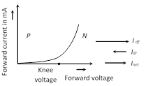
(v) Cut-in (Knee) voltage : The voltage at which the current starts to increase rapidily. For Ge it is 0.3 V and for Si it is 0.7 V.
(vi) df -diffusion dr - drift
(2) Reverse biasing : Positive terminal of the battery is connected to the N-crystal and negative terminal of the battery is connected to P-crystal
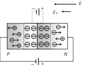
(i) In reverse biasing width of depletion layer increases
(ii) In reverse biasing resistance offered \[{{R}_{\operatorname{Re}verse}}\approx {{10}^{5}}\Omega \]
(iii) Reverse bias supports the potential barrier and no current flows across the junction due to the diffusion of the majority carriers. (A very small reverse currents may exist in the circuit due to the drifting of minority carriers across the junction)
(iv) Break down voltage : Reverse voltage at which break down of semiconductor occurs. For Ge it is 25 V and for Si it is 35 V.
(v) 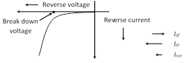


You need to login to perform this action.
You will be redirected in
3 sec

